74HC vs 74HCT vs 74LV: How to Choose the Right 74-Series Logic IC for Your Design
Compare 74HC vs 74HCT vs 74LV logic ICs: voltage thresholds, TTL compatibility, power use, and timing specs. Selection guide for engineers.
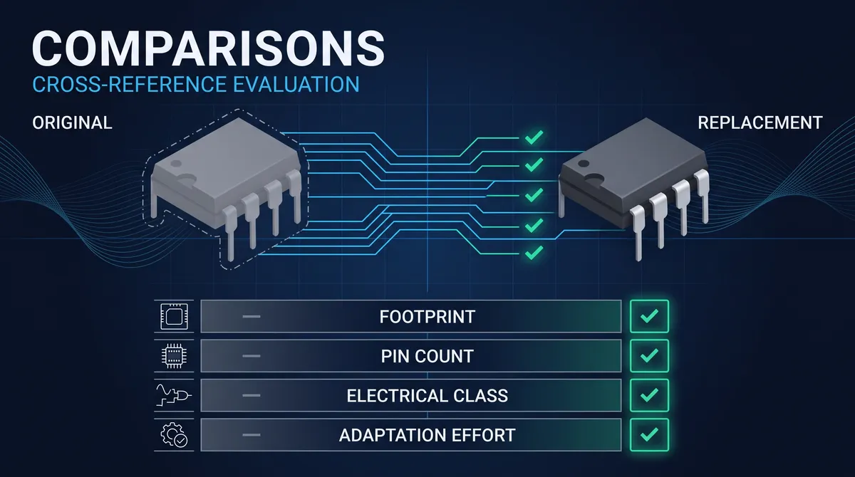
74HC vs 74HCT vs 74LV represent three of the most widely deployed families within the 74-series logic IC ecosystem, each optimized for distinct voltage domains, compatibility requirements, and power budgets. The 74HC (High-speed CMOS) operates across a 2.0V to 6.0V supply range with CMOS-level thresholds, the 74HCT variant maintains TTL-compatible 1.2V to 1.6V input thresholds despite sharing the CMOS fabrication process, and the 74LV (Low-Voltage) family targets 1.2V to 3.6V systems where reduced power consumption and faster switching at lower voltages are paramount. Choosing between these families requires understanding not only their absolute voltage specifications but also the critical interface compatibility between legacy TTL systems and modern low-power designs. Engineers selecting logic ICs must evaluate input voltage thresholds, output drive capabilities, propagation delay trade-offs, and system-level power budgets to avoid costly redesigns. This guide examines the 74HC vs 74HCT difference across electrical characteristics, application domains, and design best practices.
The 74-Series Logic IC Ecosystem: Why These Families Still Dominate Industrial and Consumer Designs
The 74-series logic family traces its origins to the 1960s with the introduction of TTL (Transistor-Transistor Logic) devices, yet the modern CMOS-based derivatives including 74HC, 74HCT, and 74LV remain among the most procured components in the global electronics supply chain. These families collectively account for billions of units shipped annually across automotive, industrial control, consumer electronics, and communication infrastructure applications. The persistence of 74-series devices stems from their perfect balance of availability, standardization, and design predictability. Every major semiconductor manufacturer—including NXP, Texas Instruments, Toshiba, ON Semiconductor, and Diodes Incorporated—produces pin-compatible 74HC, 74HCT, and 74LV devices, ensuring second-source availability that eliminates single-supplier risk. The standardized pinout and function definitions established decades ago remain unchanged, meaning engineers can swap between manufacturers without PCB redesigns. The 74HC family specifically operates at CMOS voltage levels, requiring input logic-high signals at greater than 70% of VCC for reliable operation. This characteristic makes 74HC ideal for pure CMOS systems but creates interface challenges when connecting to legacy 5V TTL circuits. The 74HCT variant resolves this incompatibility by implementing TTL-compatible input thresholds standardized at 1.2V minimum for logic-low to 1.6V minimum for logic-high recognition. Meanwhile, the 74LV family extends the voltage range downward to 1.2V minimum supply, addressing the semiconductor industry's shift toward lower operating voltages mandated by mobile and battery-powered applications. Understanding these fundamental distinctions forms the foundation for making optimal logic family selections in any electronic design.
Electrical Specifications Deep Dive: Voltage, Current, and Power Parameters
Supply Voltage Ranges and Operating Windows
The supply voltage specification represents the most fundamental differentiator between 74HC, 74HCT, and 74LV logic families. The 74HC family supports operating voltages from 2.0V at minimum through 6.0V at maximum, with 4.5V to 5.5V representing the specified test conditions for datasheet parameters. This wide voltage span allows 74HC devices to operate in both legacy 5V systems and modern 3.3V designs without modification. The 74HCT family maintains identical supply voltage requirements to 74HC, operating from 2.0V to 6.0V, which simplifies inventory management when both families appear in a single design. The 74LV family, however, targets the evolving lower-voltage ecosystem with a typical operating range of 1.2V to 3.6V. Some 74LV variants support operation down to 0.9V, though at reduced drive strength and increased propagation delay. The 74LV family often specifies a recommended operating voltage of 2.0V or 3.3V, with performance optimized at these common system voltages. When evaluating the 74HC vs 74HCT difference regarding voltage ranges, designers should note that while the absolute ranges overlap significantly, the input threshold characteristics differ dramatically despite shared supply voltage windows. The 74HC family interprets input voltages according to CMOS thresholds where VIL equals 30% of VCC and VIH equals 70% of VCC. At 5.0V operation, this means VIL ≤ 1.5V and VIH ≥ 3.5V. The 74HCT family, however, uses fixed TTL-compatible thresholds where VIL ≤ 0.8V and VIH ≥ 2.0V, regardless of VCC voltage. This distinction means a 74HCT input will reliably recognize a 3.3V signal as logic-high even when operating from a 5.0V supply, whereas a 74HC device at 5.0V VCC requires at least 3.5V for guaranteed logic-high recognition. The 74LV family typically implements CMOS thresholds scaled to its lower supply range, often with VTT-compatible options for memory interface applications. Designers must carefully review datasheet specifications for each specific device, as threshold voltages can vary between manufacturers despite shared family designations.
Input and Output Current Characteristics
Input leakage current specifications reveal the high-impedance nature of CMOS inputs and highlight subtle differences between families. The 74HC and 74HCT families specify maximum input leakage current of ±1.0µA at 25°C ambient temperature, though many commercial-grade devices achieve leakage currents below 100nA. The 74LV family often specifies slightly higher leakage current limits of ±5.0µA due to the smaller transistor geometries required for low-voltage operation, though this remains negligible for most general-purpose applications. Output current drive capability differs more significantly between families. The standard 74HC and 74HCT devices typically specify output current of ±4.0mA for low-level outputs (IOL) and ±4.0mA for high-level outputs (IOH) at 4.5V VCC, with drive capability scaling proportionally with supply voltage. At 6.0V VCC, output current can reach ±5.2mA, while at minimum 2.0V supply, drive current may drop to approximately ±1.0mA. The 74LV family generally offers reduced output drive of ±2.0mA to ±4.0mA depending on specific variant and supply voltage, reflecting the lower voltage headroom available for output switching. Bus-hold circuitry, available in certain 74HC and 74LV variants designated with the "B" suffix (such as 74HC244B), provides internal positive feedback that maintains the last valid logic state on input pins without external pull-up or pull-down resistors. This feature eliminates floating input issues in multi-drop bus applications and reduces external component count. The bus-hold current typically ranges from 10µA to 100µA, sufficient to overcome weak external pull-downs while remaining low enough to be overridden by active drivers. When evaluating 74HC vs 74HCT vs 74LV for current-intensive applications such as LED driving or bus buffering, designers should compare the absolute maximum output current specifications alongside thermal resistance characteristics to ensure adequate drive capability.
Power Consumption: Static and Dynamic Considerations
CMOS logic families exhibit two distinct power consumption components: static current resulting from input leakage and any DC paths through the input structures, and dynamic current related to output switching and input capacitance charging. The 74HC family specifies maximum quiescent supply current (ICC) of 20µA per package at 25°C, though many devices achieve 2µA to 5µA under typical conditions. This static current remains essentially constant regardless of switching frequency, making 74HC suitable for battery-powered applications that spend extended periods in standby states. Dynamic power consumption in CMOS follows the equation P = CV²f, where C represents the total switched capacitance, V represents the supply voltage, and f represents the switching frequency. This quadratic relationship between voltage and power explains the semiconductor industry's relentless drive toward lower operating voltages—the power savings from reducing VCC from 5.0V to 3.3V amount to a 56% reduction in dynamic power consumption even before accounting for reduced switched capacitance. The 74LV family, operating at 2.0V or 3.3V rather than 5.0V, delivers substantial power savings in active switching applications. At 100MHz switching frequency with 20pF load capacitance, a 74HC device at 5.0V dissipates approximately 1.0mW per switching node, while the same circuit using 74LV at 2.0V dissipates only 0.16mW—a reduction factor of over 6x. The 74HCT family exhibits similar power characteristics to 74HC under equivalent operating conditions, with the primary distinction being its TTL-compatible input thresholds that enable seamless interfacing without additional level-shifting components that would themselves consume power. Designers targeting ultra-low-power applications should consider that 74LV devices optimized for 1.2V operation can achieve quiescent currents below 1µA, making them suitable for IoT sensor nodes and portable medical devices where battery life determines product viability.
Propagation Delay and Switching Speed Performance
Typical Propagation Delay Specifications
Propagation delay represents the time interval between an input transition and the corresponding output transition, constituting a critical parameter for system timing budget allocation. The 74HC family specifies typical propagation delays of 8ns to 12ns for standard-speed variants at 4.5V VCC, with propagation delay increasing to approximately 15ns at minimum 2.0V supply voltage. High-speed 74HC variants designated with the "HC" prefix followed by additional speed gradings can achieve propagation delays as low as 5ns, though with correspondingly higher power consumption. The 74HCT family maintains propagation delay specifications comparable to 74HC, with typical values of 10ns to 15ns at 4.5V VCC. The input threshold modifications required for TTL compatibility introduce negligible additional delay compared to standard 74HC devices from the same manufacturer. The 74LV family, despite its low-voltage focus, achieves competitive propagation delays of 6ns to 12ns at 2.0V VCC, with some variants delivering sub-5ns propagation delays when operating from 3.3V supply. This impressive speed-to-power ratio results from optimized transistor structures that reduce parasitic capacitance while maintaining adequate drive capability for short-rail voltage swings. Maximum operating frequency specifications typically exceed 30MHz for 74HC and 74HCT devices and 40MHz for optimized 74LV variants, providing sufficient bandwidth for most industrial control, consumer electronics, and communication infrastructure applications. Designers working on high-speed interfaces such as memory address demultiplexing, peripheral selection, or clock distribution should verify propagation delay specifications at their specific operating voltage and temperature conditions, as performance degrades significantly at voltage extremes and elevated temperatures.
Rise Time, Fall Time, and Signal Integrity
Output transition times—the rise time (tRLH) measuring the output low-to-high transition and fall time (tRHL) measuring the high-to-low transition—affect signal integrity in ways that propagation delay alone cannot capture. The 74HC family specifies maximum rise and fall times of 15ns to 20ns for standard loads of 50pF capacitance at 4.5V VCC, though faster transitions occur with reduced load capacitance. The 74LV family achieves faster transitions at lower voltages due to the reduced voltage swing required, with typical rise and fall times of 5ns to 10ns at 3.3V operation. These faster transitions improve signal integrity in high-speed applications by reducing the time window during which outputs remain in the linear transition region where both pull-up and pull-down transistors conduct simultaneously. Undershoot and overshoot during output transitions can cause reliability issues in systems with long interconnect traces or poor impedance matching. The 74HC and 74HCT families, when operating at 5.0V, can produce output overshoot exceeding 0.5V above VCC during high-to-low transitions if inductive load effects are significant. The 74LV family, with its reduced voltage swing, produces proportionally smaller overshoot magnitudes. Designers addressing signal integrity concerns should consider adding series termination resistors at outputs driving transmission lines, implementing adequate supply decoupling with low-inductance ceramic capacitors placed close to each logic device, and minimizing trace lengths between fast-switching outputs and their destination inputs. The combined effects of propagation delay variation between individual devices, temperature coefficient of propagation delay, and supply voltage sensitivity must be incorporated into system timing margin calculations to ensure reliable operation across the full component tolerance range and environmental conditions.
Input Threshold Characteristics: The Critical Distinction
CMOS Input Thresholds Explained
The input threshold specification determines what voltage levels the logic device interprets as logic-low and logic-high, representing the fundamental difference between 74HC and 74HCT families. CMOS input thresholds scale proportionally with supply voltage, maintaining a constant fraction of VCC for noise margin optimization. The standard CMOS specification defines maximum input voltage for logic-low (VIL) at 30% of VCC and minimum input voltage for logic-high (VIH) at 70% of VCC. At 5.0V VCC, this yields VIL ≤ 1.5V and VIH ≥ 3.5V, leaving a 2.0V noise margin for each logic level. This scaling characteristic means that a 74HC device operating from 3.3V interprets input thresholds at 0.99V for VIL and 2.31V for VIH, while the same device at 2.0V VCC uses thresholds of 0.6V and 1.4V respectively. The noise margin—the difference between output drive levels and input requirement thresholds—remains proportional to supply voltage, providing approximately 30% VCC noise immunity for each logic level regardless of operating voltage. This characteristic makes 74HC ideal for systems where all components share the same supply voltage and where maximum noise immunity is required. The input structure of 74HC devices includes ESD protection diodes connected from each input to VCC and ground, which become forward-biased when input voltages exceed VCC by more than approximately 0.5V. This creates a clamping action that protects against ESD events but also introduces current flow when interfacing to higher-voltage sources. Designers must limit input voltages to VCC + 0.5V maximum to avoid excessive diode conduction and potential device damage.
TTL-Compatible Thresholds in 74HCT
The 74HCT family implements fixed input thresholds optimized for compatibility with legacy TTL logic operating at 5.0V. TTL logic families, including the original 7400 series and 74LS family, specified VIH at 2.0V minimum and VIL at 0.8V maximum, with worst-case noise margins of only 0.4V. These relatively tight thresholds reflected the bipolar transistor technology limitations of early TTL devices. The 74HCT family replicates these TTL thresholds using CMOS transistor technology, enabling direct interconnection between modern CMOS logic and existing TTL-based systems without level-shifting circuitry. The 74HCT input thresholds are specified as VIL maximum of 0.8V and VIH minimum of 2.0V, providing compatibility with both 5V TTL outputs and modern 3.3V LVTTL (Low-Voltage TTL) outputs. An LVTTL output guaranteed to swing above 2.4V will reliably be recognized as logic-high by a 74HCT input regardless of whether the 74HCT operates from 4.5V, 5.0V, or 5.5V supply. This voltage-independent threshold specification means that 74HCT devices do not exhibit the proportional threshold scaling characteristic of 74HC devices. At 5.0V VCC, the 74HCT provides approximately 1.5V noise margin for both logic levels, while at 3.3V VCC the noise margin reduces to approximately 1.3V for logic-high and 2.5V for logic-low. The input structure of 74HCT devices differs from 74HC, omitting the VCC-connected ESD protection diode to prevent current injection when input voltages exceed VCC. This modification enables 74HCT inputs to tolerate input voltages up to 7.0V absolute maximum regardless of VCC voltage, though the devices must still operate within their specified 2.0V to 6.0V supply range. This tolerance allows 74HCT devices to interface with 5.0V signaling even when operating from 3.3V supplies, though designers should verify this capability in specific device datasheets as it varies between manufacturers and device types.
Application Domains: Selecting the Right Family for Your System
Automotive and Industrial Control Applications
The automotive and industrial sectors represent major application domains where 74HC and 74HCT families dominate due to their proven reliability, extended temperature ranges, and multi-source availability. Automotive applications require logic devices rated for operation from -40°C to +125°C junction temperature, with 74HC and 74HCT variants available in automotive temperature grades from most major suppliers. The 74HC family serves as the standard choice for new automotive designs operating from 5.0V or 3.3V supplies, where all system components share common voltage domains. Body control modules, instrument clusters, infotainment systems, and advanced driver assistance systems (ADAS) incorporate 74HC gates, flip-flops, latches, and buffer devices throughout their digital logic implementations. The 74HCT family finds application in legacy automotive platforms where existing control units implement TTL-level signaling, enabling new 74HCT-based circuits to interoperate with installed base equipment without interface modifications. Industrial control applications, including programmable logic controllers (PLCs), motor drives, and process automation equipment, similarly deploy 74HC and 74HCT devices in both new designs and retrofits of existing systems. The wide availability of these families in through-hole DIP packages for legacy board assembly and surface-mount SOP/SSOP/TSSOP packages for modern assembly processes ensures compatibility across the full spectrum of industrial manufacturing capabilities. Designers should verify that selected devices carry relevant industry certifications such as AEC-Q100 for automotive applications, IEC 60730 for safety-related industrial controls, and conflict mineral reporting documentation for European Union RoHS compliance. The extended product lifecycle support offered by multiple manufacturers for 74HC and 74HCT families provides supply chain continuity assurance that industrial equipment manufacturers require for long-lifecycle products.
Consumer Electronics and Computing Applications
Consumer electronics and computing applications increasingly favor 74LV and low-voltage CMOS logic families due to power consumption constraints and the industry-wide transition toward lower supply voltages. Desktop computers, servers, and networking equipment operating from 3.3V and 2.5V supply rails implement 74LV devices for level translation, bus buffering, and control signal distribution. The 74LV family operates efficiently at these reduced voltages while maintaining compatibility with legacy 5.0V signaling through careful interface design. Notebook computers and tablet devices, constrained by thermal limits and battery life requirements, implement 74LV logic extensively throughout their power management, interface, and peripheral control circuits. The low quiescent current of 74LV devices, often specified below 1µA for individual gates, becomes significant when dozens of logic devices remain active during system standby modes. Consumer audio equipment, including digital signal processing boards, interface converters, and control panels, deploy 74HC and 74LV devices for signal routing, switching, and status indication. The immunity of CMOS inputs to floating conditions and the availability of Schmitt trigger variants for noisy signal environments make these families suitable for audio applications where electromagnetic interference from power supply switching can corrupt logic signals. Mobile devices and battery-powered equipment represent the extreme end of the power consumption spectrum, often implementing custom ASICs and specialized low-voltage logic rather than standard 74LV devices. However, the 74LV family continues to serve these applications through support functions such as power sequencing, battery monitoring, and external peripheral control where standard logic provides cost-effective solutions unavailable in custom silicon. The rapid pace of consumer electronics product development benefits from the immediate availability of 74-series samples and production quantities from multiple distributors, enabling design schedules that cannot accommodate custom ASIC development timelines.
Communication Infrastructure Applications
Communication infrastructure equipment spanning cellular base stations, fiber optic transmission systems, wireless access points, and network switching equipment deploys 74HC, 74HCT, and 74LV logic in various system locations based on voltage domains and interface requirements. Central office and data center equipment typically operates from 48V nominal supply rails with distributed conversion to 3.3V and 2.5V for digital logic, making 74LV devices the primary logic family for new designs. The high reliability, proven long-term availability, and multi-vendor sourcing of 74-series devices align with the 15-25 year deployment lifetimes typical of communication infrastructure equipment. Timing-critical functions such as clock distribution, frame synchronization, and signal conditioning benefit from the predictable propagation delay specifications of 74HC and 74HCT devices operating at 5.0V where available drive current provides excellent edge transition times. The 74HCT family enables interface between new low-voltage equipment and legacy TDM (Time Division Multiplexing) systems that implemented TTL signaling, maintaining interoperability during technology transition periods. Optical transport equipment operating at 10Gbps, 25Gbps, and 100Gbps data rates requires logic devices with propagation delays below 5ns for timing management, achievable with high-speed 74HC and certain 74LV variants at elevated supply voltages. Designers should carefully review the frequency response characteristics of selected devices, as some logic families exhibit increased propagation delay at elevated temperatures that can compromise margin in high-density equipment where ambient temperatures can reach 70°C or higher.
Voltage Level Translation: Interfacing Between Logic Families
Bidirectional Level Translation with 74HC, 74HCT, and 74LV
Modern electronic systems frequently require voltage level translation between circuits operating at different supply voltages, and 74-series devices provide several proven approaches to this challenge. The simplest level translation scenario involves connecting a 3.3V output to a 5.0V input. For 74HC inputs operating from 5.0V, a 3.3V output typically fails to meet the 70% VCC (3.5V) requirement for guaranteed logic-high recognition. A 74HCT input solves this problem directly, as its fixed 2.0V VIH threshold accepts 3.3V signaling without modification. This makes 74HCT an ideal choice for interfacing 3.3V microcontrollers to 5.0V peripherals, memory devices, or legacy control circuits. For connecting 5.0V outputs to 3.3V inputs, designers must ensure that the 5.0V signal does not exceed the maximum input rating of the receiving device. Most 3.3V logic specifies maximum input voltages of 3.6V or VCC + 0.3V, making direct 5.0V connection potentially damaging. A simple voltage divider reduces the 5.0V signal to safe levels but degrades signal integrity and increases transition times. Alternatively, 74LV devices designed with 5V-tolerant inputs accept 5.0V signaling while operating from 3.3V supply, providing a single-component solution for unidirectional translation. Bidirectional level translation for data buses such as SPI, I2C, or GPIO expanders requires more sophisticated approaches. A standard technique uses a dual-supply buffer such as the 74LVX245 or 74LVCH245 with separate VCCA and VCCB supply pins rated for different voltages. When VCCA connects to 3.3V and VCCB connects to 5.0V, the device translates signals between the two voltage domains in both directions automatically. For lower-speed applications, a simple MOSFET-based translator using BSS138 or similar small-signal MOSFETs provides cost-effective bidirectional translation for open-drain buses such as I2C.
Design Guidelines for Mixed-Voltage Systems
Designing robust mixed-voltage systems requires careful attention to power-up sequencing, input protection, and output drive compatibility. The preferred approach sequences power supplies from highest voltage to lowest voltage, ensuring that no device receives input signals before its supply voltage reaches the minimum operating specification. This prevents latch-up conditions and input leakage issues that occur when input structures see voltages before proper bias is established. Many 74HC and 74HCT devices include internal power-up reset circuits that place outputs in a defined state during voltage ramp, preventing bus contention during system initialization. Output drive compatibility between logic families depends on the input threshold specifications of receiving devices. A 74HC output driving a 74HCT input presents no issues, as the 74HC output swings to VCC (guaranteed above 3.5V at 5V operation) which exceeds the 74HCT VIH of 2.0V. However, a 74HCT output driving a 74HC input at 5.0V requires the output to reach 3.5V for guaranteed recognition, and while standard 74HCT outputs do achieve this level, the noise margin is reduced compared to 74HC-to-74HC connections. When mixing 74HC and 74LV devices, designers should verify that the reduced output voltage swing of 74LV devices operating at 2.0V or 3.3V meets the input requirements of 74HC devices. A 74LV output at 3.3V is insufficient to drive a 74HC input requiring 3.5V at 5.0V operation, necessitating either level-shifting or operating all devices from compatible supply voltages. The safest mixed-voltage design guidelines recommend grouping devices by supply voltage, implementing level translation at domain boundaries, and verifying all interface signal levels across worst-case operating conditions including minimum VCC, maximum temperature, and maximum load current.
Thermal Management Considerations
Power Dissipation and Junction Temperature
Logic ICs dissipate power through both quiescent current flow and dynamic switching losses, with total dissipation determining the device junction temperature relative to ambient environment. The junction-to-ambient thermal resistance (θJA) of standard 74HC and 74HCT packages ranges from 80°C/W for DIP packages to 150°C/W for small-outline surface-mount packages without thermal vias, declining to 40°C/W to 60°C/W with adequate copper pad area and thermal vias. The 74LV family typically exhibits lower power dissipation due to reduced operating voltage but may have slightly higher thermal resistance due to smaller die sizes. Calculating junction temperature requires multiplying total power dissipation by thermal resistance and adding ambient temperature. For a 74HC device in a SOP package with θJA of 120°C/W dissipating 10mW in a 70°C ambient environment, junction temperature equals 70°C plus 1.2°C, well within the 150°C maximum rating. However, densely populated boards with poor airflow can experience ambient temperatures exceeding 85°C in industrial environments, and high-speed logic devices switching at megahertz frequencies with significant load capacitance can dissipate tens of milliwatts per package, requiring careful thermal analysis. The maximum ambient temperature specification in datasheets assumes a specific thermal environment and load condition; actual system ambient limits may be lower depending on power dissipation and thermal resistance in the actual mounting configuration. Designers should measure or estimate the actual thermal resistance of their board layout using finite element analysis or empirical testing, then verify that junction temperatures remain below 125°C for commercial temperature rated devices and 150°C for industrial temperature rated devices under worst-case operating conditions.
Thermal Design Best Practices
Effective thermal management for 74-series logic circuits begins with minimizing power dissipation through appropriate family selection and circuit design. Operating 74HC devices from 3.3V rather than 5.0V reduces dynamic power consumption by approximately 56% while simultaneously reducing thermal stress on the device. The 74LV family extends this advantage further, operating at 2.0V or 1.8V where system architecture permits. Reducing load capacitance through shorter traces, smaller pull-up resistors, and elimination of unnecessary fan-out minimizes switching-related power dissipation. When power dissipation exceeds thermal capacity, adding thermal relief copper pads beneath packages, implementing thermal vias to spread heat to internal board layers, and improving airflow through component placement and optional fans can maintain junction temperatures within safe limits. For high-density systems where thermal constraints limit logic density, designers should consider upgrading to ABT (Advanced BiCMOS Technology) or ALVC (Advanced Low-Voltage CMOS) families that deliver higher drive capability and faster switching from lower supply voltages, though at increased cost per device. Temperature monitoring using thermal sensors placed near heat-generating components enables dynamic thermal management through throttling or fan speed control in safety-critical applications. The long-term reliability impact of junction temperature follows an exponential relationship with absolute temperature according to the Arrhenius equation, with every 10°C increase in junction temperature approximately halving device lifetime. This relationship makes thermal management not merely a performance consideration but a fundamental reliability requirement for equipment expected to operate for tens of thousands of hours.
Reliability and Quality Considerations
Failure Modes and Mechanism
Understanding the failure mechanisms of 74-series logic devices enables designers to implement circuit techniques that improve system reliability. Oxide breakdown, the primary wear-out mechanism in MOSFET-based CMOS logic, occurs when electric field strength across the gate oxide exceeds approximately 10MV/cm. Modern 74HC, 74HCT, and 74LV devices manufactured with 0.5µm to 0.35µm process technologies include robust ESD protection structures rated for 2kV Human Body Model (HBM) and 200V Machine Model (MM) discharge events. Designers should implement additional protection circuitry for applications exposed to higher ESD threat levels such as automotive ignition systems, industrial motor controls, or outdoor equipment. Latch-up, a potentially destructive condition where parasitic thyristor structures within CMOS devices become activated, can destroy devices when supply current exceeds 100mA. Latch-up triggers include input voltages exceeding VCC, output voltages exceeding VCC, and supply voltage transients. The 74HCT family offers inherent latch-up immunity for input overvoltage conditions due to the absence of VCC-connected ESD diodes, while 74HC and 74LV devices require careful attention to absolute maximum ratings to avoid latch-up events. Electromigration, the gradual displacement of metal atoms in conductors due to high current density, affects interconnections within logic devices when current density exceeds approximately 1mA/µm². Standard 74-series devices maintain safe current densities well below electromigration thresholds for normal operating conditions, but designs driving low-impedance loads or implementing test modes with elevated current should verify compliance with absolute maximum current specifications.
Quality and Reliability Grades
Semiconductor manufacturers offer 74HC, 74HCT, and 74LV devices in multiple quality grades tailored to specific application requirements and environmental conditions. Commercial temperature range devices rated for 0°C to +70°C ambient operation serve cost-sensitive consumer electronics and computer applications where failure consequences are limited. Industrial temperature range devices rated for -40°C to +85°C provide expanded environmental capability for industrial control, instrumentation, and telecommunications applications. Automotive temperature range devices rated for -40°C to +125°C junction temperature undergo additional screening and qualification testing per AEC-Q100 standards, including temperature cycling, unbiased accelerated life testing, and electrical verification at temperature extremes. Military-grade 74-series devices meeting MIL-PRF-38535 QML specifications serve aerospace and defense applications requiring extended reliability assurance. The additional cost of automotive-grade devices over commercial equivalents typically amounts to 20% to 50% depending on package type and manufacturer, a modest premium for applications where field failures carry significant warranty, recall, or liability costs. Designers should verify that selected devices carry full manufacturing date codes enabling lot traceability, that datasheets specify the quality grade rather than merely the temperature range, and that supplier quality management systems conform to ISO 9001 or equivalent standards. Counterfeit 74-series devices remain a concern in the global electronics supply chain, making authorized distribution channels and supplier verification essential for reliability-critical applications.
Design Checklist and Decision Matrix
Family Selection Criteria Summary
Selecting between 74HC, 74HCT, and 74LV requires systematic evaluation of system requirements against family capabilities. The following decision criteria enable rapid family selection for most applications. If the system operates exclusively from a single voltage domain at CMOS levels (3.3V, 5.0V, or similar), 74HC provides maximum noise margin and input compatibility within that voltage domain. If the system requires interface to legacy 5V TTL signals or LVTTL outputs from microcontrollers and memory devices, 74HCT simplifies the interface without additional level-shifting components. If power consumption is the primary constraint and all interfacing signals operate at 3.3V or lower, 74LV minimizes active and standby power dissipation. If the system requires operation below 2.0V supply voltage, 74LV represents the only standard 74-series option among these three families. If output drive current requirements exceed 4.0mA at standard supply voltages, verify specific device drive capabilities as they vary by function and manufacturer. If the application requires extended temperature operation above +85°C ambient, verify automotive or industrial temperature grades are available for the specific device function required. If the system design mandates single-source avoidance, confirm that at least two manufacturers produce pin-compatible equivalents for all selected devices.
Common Design Errors to Avoid
Several recurring design errors cause reliability issues and field failures in 74-series implementations. Connecting 5.0V outputs directly to 74HC inputs operating from 3.3V supply violates absolute maximum ratings and can cause immediate failure or accelerated degradation. Always implement level translation or verify 5V-tolerant input specifications before such connections. Assuming 74HC and 74HCT are interchangeable overlooks the critical input threshold difference—a 74HC input may fail to recognize a 3.3V signal as logic-high when operating from 5.0V supply. Relying on 74HC output levels to drive 74HCT inputs in new designs wastes noise margin unnecessarily. Neglecting load capacitance effects causes timing violations in high-speed designs—every 50pF of load capacitance adds approximately 10ns to transition times. Distributing outputs across long traces or through connectors without series termination produces ringing that can exceed logic thresholds and cause intermittent failures. Operating at minimum supply voltage with maximum load current and elevated temperature produces propagation delays at the datasheet limits, potentially violating system timing margins. Skipping input transition time requirements—some 74HC devices require input rise and fall times below 500ns to avoid oscillation—causes spurious switching in noisy environments. Using decoupled outputs without pull-up or pull-down resistors for unconnected inputs allows floating inputs to consume excessive current in certain input configurations. Reviewing designs against this error checklist before release can prevent costly respins and field failures.
Conclusion: Making the Right Choice for Your Application
The selection between 74HC vs 74HCT vs 74LV ultimately depends on understanding the specific requirements of your system including supply voltage, interface compatibility, power constraints, and environmental conditions. The 74HC family remains the workhorse choice for pure CMOS systems operating from single voltage domains, offering maximum noise margins and proven compatibility across manufacturers. The 74HCT variant provides essential TTL compatibility that simplifies interface design when connecting to legacy systems, microcontrollers, or other components that output LVTTL signal levels. The 74LV family addresses the industry trend toward lower operating voltages, delivering significant power savings in battery-powered and thermally constrained applications while maintaining competitive speed performance. PinCompatible offers comprehensive inventory of 74HC, 74HCT, and 74LV devices from multiple manufacturers with same-day shipping and competitive pricing. Our technical support team can assist with cross-reference searches, alternative device recommendations, and design review questions for complex mixed-voltage systems. Explore our complete selection of 74-series logic ICs to find the optimal devices for your next design project.
Not sure which sensor fits your project?
Talk to our mmWave application engineers for a free consultation.
Specify your hotel project with our engineers
Send your room count, ceiling type, and protocol preference. We will return a sample plan and quote within 24 business hours.
- Move from general guidance into a product or application discussion.
- Use RFQ when pricing, drawings, MOQ, or launch timing needs structure.
- Keep a direct contact path visible for fast clarifications and handoff.