74HC245 vs SN74HC245: Octal Bus Transceiver Pin-to-Pin Replacement Guide
A comprehensive guide comparing 74HC245 and SN74HC245 octal bus transceivers, covering pin-to-pin compatibility, electrical specs, and replacement strategies for industrial applications.
74HC245 vs SN74HC245: Octal Bus Transceiver Pin-to-Pin Replacement Guide
The 74HC245 is a widely adopted octal bus transceiver from the 74HC logic family, operating at supply voltages between 2V and 6V with propagation delays of approximately 8-15ns at 5V VCC. The SN74HC245 variant, manufactured by Texas Instruments and other authorized semiconductor suppliers, offers functionally identical pinout configurations and electrical characteristics, enabling direct pin-to-pin replacement across most industrial and consumer electronics applications. The key distinction lies in manufacturer-specific quality certifications, temperature grade offerings, and availability tiers rather than core functionality. Typical deployments include microprocessor bus buffering, memory address line expansion, and peripheral interface isolation in automotive control systems, industrial automation controllers, and communication equipment operating at frequencies up to 20MHz. Selection between these variants requires evaluation of datasheet specifications, MSL rating requirements, and supply chain continuity considerations.
Understanding Octal Bus Transceivers: The 74HC245 Architecture
Octal bus transceivers represent a fundamental building block in digital system design, serving as bidirectional buffers that enable controlled data flow between two bus segments while providing electrical isolation and signal conditioning. The 74HC245 family specifically implements an octal configuration, meaning it contains eight identical transceiver channels within a single 20-pin package, making it exceptionally efficient for applications requiring simultaneous handling of multi-bit data buses such as 8-bit microprocessors, memory interfaces, or parallel communication protocols.
The architecture of the 74HC245 centers on a direction control mechanism that determines whether data flows from port A to port B or vice versa. This bidirectional capability proves essential in systems where bus mastership changes dynamically, such as in microprocessor read-write cycles or shared peripheral interfaces. The device incorporates output enable functionality that allows all outputs to be placed in a high-impedance state, effectively disconnecting the transceiver from both buses without requiring power-down of the device itself. This three-state output design enables multiple transceivers or other bus drivers to share common data lines without contention, a critical requirement in multiplexed bus architectures.
Each channel within the 74HC245 functions as an independent buffer with consistent propagation delay characteristics, ensuring signal integrity across all eight data lines simultaneously. The HC (High-speed CMOS) technology node delivers significantly improved speed-power product compared to earlier CMOS families while maintaining full CMOS input compatibility. This means the device can interface directly with both legacy TTL logic operating at 5V and modern CMOS circuits without additional level shifting, provided voltage compatibility requirements are met. The fan-out capability allows each output to drive multiple TTL-equivalent loads, supporting typical bus configurations without external buffering.
The internal construction employs CMOS transmission gate topology for the data path, with direction control implemented through complementary MOSFET pairs that activate appropriate signal routing paths. This design minimizes ON resistance while preventing shoot-through currents that could occur if both directions were simultaneously active. The direction pin (DIR) and output enable pin (OE) provide independent control over data flow direction and bus connectivity, giving designers precise management over the transceiver's operating mode. When OE is HIGH, all outputs enter the high-impedance state regardless of the DIR setting, providing a complete disconnect mechanism.
Thermal considerations in the 74HC245 design address the reality that eight outputs switching simultaneously can generate substantial transient currents during state changes. The device incorporates internal damping resistors that limit peak di/dt during switching transients, reducing electromagnetic interference and preventing excessive ground bounce on the package pins. This built-in filtering proves particularly valuable in noisy industrial environments where conducted and radiated emissions must meet regulatory standards such as CISPR 22 or FCC Part 15 requirements. The thermal performance also supports continuous operation at the maximum specified ambient temperature without external heat sinking in most typical applications.
Pin Configuration and Pinout Analysis for Direct Replacement
The 74HC245 and SN74HC245 share a common 20-pin package configuration standardized across the semiconductor industry, enabling straightforward pin-to-pin replacement in existing designs. Understanding this pinout in detail proves essential for replacement planning and verification, as subtle differences in pin assignments between manufacturers could cause catastrophic failures if overlooked. The standard package options include TSSOP-20, SOIC-20, DIP-20, and various other surface-mount configurations, all sharing identical pin assignments for functional pins while potentially varying in thermal pad or exposed pad provisions.
Pin 1 serves as the direction control input (DIR), determining whether data flows from port A to port B or from port B to port A. When DIR is HIGH (connected to VCC), data propagates from pins A1 through A8 to corresponding B1 through B8 outputs. When DIR is LOW (connected to ground), the data path reverses, with B1 through B8 becoming inputs and A1 through A8 becoming outputs. This single-pin control allows simple microprocessor or microcontroller GPIO control over bus direction without requiring complex sequencing logic. The DIR input features standard CMOS input characteristics with defined logic thresholds at approximately 30% and 70% of VCC for the HC family.
Pins 2 through 9 implement the A bus interface, functioning as bidirectional data pins when operating in the A-to-B direction or as outputs when operating in B-to-A direction. These pins connect directly to one side of the system bus, typically the local microprocessor or controller side in most applications. Each A pin incorporates a pull-down resistor internally, ensuring defined logic levels when pins are left floating, though external termination may be required for noise-sensitive high-speed applications. The A port also serves as the reference for input threshold calculations when receiving data from the B side during B-to-A operation.
Pins 10 through 17 form the B bus interface, mirroring the A port functionality but on the opposite side of the transceiver. The B port typically connects to external peripherals, expansion connectors, or secondary bus segments that may experience more electrical noise or require additional protection. In the SN74HC245 variant from Texas Instruments, the B port includes enhanced ESD protection structures exceeding 2kV HBM (Human Body Model) and 200V MM (Machine Model) specifications, providing robustness against electrostatic discharge events during handling and assembly.
Pin 19 functions as the output enable (OE) control, active LOW in the standard 74HC245 configuration. When OE is pulled LOW, the transceiver operates normally according to the DIR setting. When OE is pulled HIGH, all eight bidirectional pins enter a high-impedance state, effectively disconnecting both ports from the internal transceiver circuitry. This enable functionality proves critical for bus sharing applications where multiple transceivers or drivers may contend for the same physical bus segments. Proper sequencing of OE relative to DIR prevents bus contention conditions that could damage devices or corrupt data.
Pin 20 provides VCC connection, with the 74HC245 supporting operation from 2V to 6V supply rails. The SN74HC245 datasheet specifies absolute maximum ratings of 7V, with recommended operating ranges between 2V and 6V for specified performance. Decoupling capacitors of 0.1µF minimum should be placed physically close to the VCC pin and ground plane to provide high-frequency current demands during output switching. For applications with long VCC traces or additional current requirements from other devices on the same rail, additional bulk capacitance may improve signal integrity and reduce VCC bounce during simultaneous switching events.
Pin 10 connects to ground (GND), establishing the reference point for all logic thresholds and providing the return path for supply current. The ground pin placement on the corner of the package (opposite VCC at pin 20) follows standard practice for minimizing inductive voltage drops between supply and ground during transient current events. Board designers should ensure adequate ground plane coverage beneath the device and connect the GND pin to the primary system ground through multiple vias if using multi-layer PCB constructions.
| Pin Number | Pin Name | Function | Direction Control |
|---|---|---|---|
| 1 | DIR | Direction Control | Input |
| 2 | A1 | Bus A Bit 1 | Bidirectional |
| 3 | A2 | Bus A Bit 2 | Bidirectional |
| 4 | A3 | Bus A Bit 3 | Bidirectional |
| 5 | A4 | Bus A Bit 4 | Bidirectional |
| 6 | A5 | Bus A Bit 5 | Bidirectional |
| 7 | A6 | Bus A Bit 6 | Bidirectional |
| 8 | A7 | Bus A Bit 7 | Bidirectional |
| 9 | A8 | Bus A Bit 8 | Bidirectional |
| 10 | GND | Ground | Power |
| 11 | B8 | Bus B Bit 8 | Bidirectional |
| 12 | B7 | Bus B Bit 7 | Bidirectional |
| 13 | B6 | Bus B Bit 6 | Bidirectional |
| 14 | B5 | Bus B Bit 5 | Bidirectional |
| 15 | B4 | Bus B Bit 4 | Bidirectional |
| 16 | B3 | Bus B Bit 3 | Bidirectional |
| 17 | B2 | Bus B Bit 2 | Bidirectional |
| 18 | B1 | Bus B Bit 1 | Bidirectional |
| 19 | OE | Output Enable (Active LOW) | Input |
| 20 | VCC | Supply Voltage | Power |
Electrical Specifications: A Comprehensive Comparison
Understanding the electrical characteristics of both the generic 74HC245 and the SN74HC245 from Texas Instruments requires examining multiple specification categories including DC parameters, AC timing characteristics, and power consumption figures. While the fundamental logic function remains identical between variants, subtle differences in process technology, design margin, and characterization methodology can produce variations in published specifications that affect system-level design margins.
The supply voltage range for both devices spans 2V to 6V, with full specification compliance guaranteed across this entire range for most parameters. At the minimum 2V supply, the 74HC245 family maintains CMOS-compatible output levels while supporting reduced power consumption for battery-powered applications. Operation at 6V provides maximum noise margins and drive strength, beneficial in electrically noisy industrial environments with significant ground bounce or supply transients. The SN74HC245 specifically characterizes power supply current (ICC) at both minimum and maximum supply voltages, with typical quiescent current of 80µA at 25°C ambient temperature.
Input voltage specifications define the logic threshold points that determine when the device recognizes a HIGH or LOW input state. For the HC family at 5V operation, VIH (minimum HIGH input voltage) is specified at 3.5V, while VIL (maximum LOW input voltage) is specified at 1.5V, yielding a robust 1V noise margin on each side of the transition region. The SN74HC245 datasheet provides detailed input threshold curves across the full supply voltage range, enabling designers to calculate appropriate noise margins for their specific VCC conditions. Input leakage current (II) remains below 1µA across the operating temperature range, ensuring minimal loading on driving circuits.
Output drive capability represents a critical specification for bus transceiver applications where the device must source or sink current to multiple loads. Both the 74HC245 and SN74HC245 specify output current of ±6mA at 4.5V VCC, with proportional scaling at other supply voltages. This drive strength enables direct connection to multiple standard TTL or CMOS inputs without external buffering. The output voltage specifications (VOH minimum of 3.84V and VOL maximum of 0.33V at 4.5V VCC and 6mA load) confirm full CMOS output level compliance, ensuring compatibility with subsequent logic stages. Short-circuit output current (IOS) is characterized but should not be sustained in normal operation.
Propagation delay specifications determine the maximum operating frequency and signal latency through the transceiver. The SN74HC245 datasheet specifies typical propagation delays of 12ns at 5V VCC with worst-case values of 20ns across the full temperature range of -40°C to +85°C (or extended -40°C to +125°C for automotive grades). The tPLH and tPHL specifications (propagation delay low-to-high and high-to-low respectively) remain well-matched, preventing asymmetric duty cycle distortion in high-speed data applications. Enable and disable times (tLZ, tHZ, tZL, tZH) characterize the transition time to and from high-impedance states, critical for bus arbitration timing.
Input capacitance (CI) specifications of approximately 3pF for each input pin determine the loading effect on driving circuits and affect signal integrity at high frequencies. The I/O pin capacitance (CIO) of approximately 5pF represents the total capacitance seen by the bus when the pin is configured as an input or high-impedance state. These parasitic capacitances, combined with trace inductances, create resonant circuits that can produce overshoot and undershoot during fast switching edges. The 74HC245 incorporates input clamping diodes that provide ESD protection but also limit negative-going transients to approximately -0.5V during normal operation.
Power consumption in the 74HC245 family comprises both static and dynamic components. Static current (ICC) flows primarily through the input protection networks and any partial conduction in the output stage, with typical values below 80µA at quiescent conditions. Dynamic current consumption increases with switching frequency and load capacitance, following the relationship ICC = ICCQ + CVCCf where C represents total switched capacitance and f represents switching frequency. At maximum specified frequency of approximately 50MHz, dynamic currents can exceed 10mA, necessitating proper supply decoupling and thermal management considerations.
| Parameter | 74HC245 Generic | SN74HC245 TI | Unit | Test Condition |
|---|---|---|---|---|
| VCC Operating Range | 2.0 - 6.0 | 2.0 - 6.0 | V | - |
| ICC (Quiescent) | < 80 | < 80 | µA | VCC=6V, VIN=VCC/GND |
| II (Input Leakage) | < 1 | < 1 | µA | VCC=6V |
| VIH (Min HIGH Input) | 3.5 | 3.5 | V | VCC=4.5V |
| VIL (Max LOW Input) | 1.5 | 1.5 | V | VCC=4.5V |
| VOH (Min HIGH Output) | 3.84 | 3.84 | V | VCC=4.5V, IOH=-6mA |
| VOL (Max LOW Output) | 0.33 | 0.33 | V | VCC=4.5V, IOL=6mA |
| tPD (Propagation Delay) | 8-20 | 12 (typ), 20 (max) | ns | VCC=5V, CL=50pF |
| tEN (Enable Time) | 20-35 | 25 (typ), 35 (max) | ns | VCC=5V |
| CIN (Input Capacitance) | 3 | 3 | pF | VCC=0V |
| CIO (I/O Capacitance) | 5 | 5 | pF | VCC=5V |
Performance Characteristics in Real-World Applications
Evaluating the practical performance of the 74HC245 and SN74HC245 in real-world applications requires understanding how datasheet specifications translate to system behavior under actual operating conditions. Temperature extremes, supply voltage variations, and load conditions all affect the margin between theoretical specifications and observed performance, potentially creating reliability issues in field-deployed equipment if not properly accounted for during design.
Temperature effects on 74HC245 operation manifest across multiple parameter dimensions, with propagation delay increasing approximately 20-30% when transitioning from 25°C to the maximum rated temperature of 85°C or 125°C. This temperature coefficient becomes significant in applications requiring precise timing margins, such as memory interface address and data bus timing. The SN74HC245 datasheet provides temperature derating curves for output current capability, showing that drive strength decreases approximately 20% at the high temperature extreme compared to room temperature operation. Designers should verify that minimum noise margins remain acceptable when accounting for these temperature variations.
Supply voltage regulation quality directly impacts 74HC245 performance, particularly in systems where multiple logic devices share common supply rails. Voltage drops during simultaneous switching events can temporarily reduce VCC below specified thresholds, causing increased propagation delays and potentially corrupted data if threshold violations occur during critical setup or hold time windows. Decoupling capacitor placement guidelines recommend 0.1µF ceramic capacitors placed within 3mm of the device VCC pin, with additional bulk capacitance of 10µF or more on the supply plane to absorb transient current demands. For systems with long PCB traces between the power supply and 74HC245, impedance of the supply distribution network should be analyzed to ensure adequate high-frequency current delivery.
Signal integrity considerations in high-speed applications reveal limitations that may not be apparent from standard datasheet specifications. The 74HC245 output stage, while providing adequate drive for logic level compatibility, exhibits finite output impedance that interacts with load capacitance and trace characteristics to produce transmission line effects at frequencies above approximately 20-30MHz. Reflections from unmatched transmission line terminations can cause overshoot exceeding absolute maximum ratings if not properly managed. Board designers targeting frequencies above 20MHz should consider controlled-impedance routing, series termination resistors, or selection of higher-speed transceiver families designed specifically for such applications.
Electrostatic discharge resilience varies between manufacturers, with the SN74HC245 typically incorporating enhanced protection structures compared to generic 74HC245 parts from secondary sources. The Texas Instruments specification of >2kV HBM and >200V MM provides adequate protection for most handling and assembly conditions, but applications in extremely ESD-prone environments may require additional external protection components. Generic parts may specify lower ESD ratings or provide no guaranteed specification, creating risk in applications where ESD events are likely. Verification of ESD specifications with datasheet review remains essential before committing to any 74HC245 replacement alternative.
Operating lifetime and reliability projections for the 74HC245 family indicate mean time between failures (MTBF) exceeding 1 million hours under typical operating conditions, with failure modes primarily related to oxide degradation or wire bond fatigue over extended thermal cycling. The SN74HC245 carries extended reliability characterization data in its datasheet, including failure rate projections at various junction temperatures using industry-standard models. For applications requiring extended product lifetimes exceeding 10 years, selection of automotive-grade SN74HC245 variants with extended temperature range and enhanced process controls may provide better long-term reliability despite higher unit costs.
Application Scenarios: When to Choose the SN74HC245
Understanding the specific application contexts where the SN74HC245 provides advantages over generic 74HC245 alternatives enables informed selection decisions that optimize cost-performance tradeoffs for each design. Not every application requires the enhanced specifications and quality grades available from major semiconductor manufacturers, but certain use cases clearly benefit from the additional engineering margin and supply chain reliability that branded components provide.
Industrial control systems operating in factory environments represent a primary application category where SN74HC245 selection proves advantageous. These applications typically require extended temperature operation (-40°C to +85°C minimum), long product lifecycle support exceeding 10 years, and consistent device-to-device performance for multi-system deployments. The SN74HC245 from Texas Instruments provides detailed automotive and industrial temperature grade options with full characterization across these ranges, along with single-source supply chain commitments that simplify long-term procurement planning. Generic 74HC245 parts may not support these temperature grades or may exhibit wider parameter distributions that affect system-level timing margins.
Automotive electronics applications impose the most stringent requirements on logic device selection, with AEC-Q100 qualification mandatory for safety-critical functions and strong recommendations for other in-vehicle systems. The SN74HC245-Q1 variant specifically undergoes AEC-Q100 testing including accelerated life testing, electrostatic discharge characterization, and latch-up testing, providing documented compliance with automotive quality standards. Generic 74HC245 parts lack this qualification, making them unsuitable for automotive deployments regardless of functional compatibility. The cost premium for automotive-grade logic typically ranges from 50% to 200% compared to commercial-grade equivalents, but provides risk mitigation against field failures that could far exceed the component cost difference.
Consumer electronics manufacturing at high volumes benefits from SN74HC245 selection through improved availability and pricing stability from established distribution channels. Major semiconductor manufacturers maintain capacity allocation commitments for automotive and industrial customers, ensuring supply availability even during market shortages that commonly affect commodity logic devices. Generic 74HC245 sources may disappear or become unreliable during demand spikes, creating production line stoppages that cost far more than component price differences. Volume pricing from authorized distributors often approaches parity with generic sources when total cost of supply disruption risk is properly accounted.
Medical device manufacturing operates under FDA quality system requirements that favor traceable, documented component sources with established reliability histories. The SN74HC245 provides datasheet specifications with guaranteed minimum and maximum values, statistical process control data, and manufacturer quality certifications that simplify regulatory compliance documentation. Generic parts may lack complete characterization data or may exhibit batch-to-batch variations that complicate design validation and re-verification requirements. For Class II and Class III medical devices requiring 510(k) or PMA submissions, component selection decisions should involve quality engineering review to ensure regulatory compliance.
Communication infrastructure equipment, including base station hardware and network switching equipment, requires logic devices that support extended temperature operation and provide consistent timing characteristics across large system deployments. The SN74HC245 characterization includes propagation delay distribution data across production lots, enabling statistical timing analysis that accounts for device-to-device variation. This data supports robust design margin calculations that ensure system-level timing compliance at the specified operating temperature range. Generic 74HC245 datasheets of
Identifying and Sourcing a 74HC245 Replacement Alternative
When the original 74HC245 component becomes unavailable through standard distribution channels, engineering teams must evaluate replacement alternatives that maintain functional and electrical compatibility while meeting application requirements. The semiconductor industry offers multiple paths to securing functional replacements, each with distinct tradeoffs in availability, cost, specification compliance, and supply chain risk that require careful evaluation before final selection.
Direct pin-to-pin compatible replacements represent the first consideration when sourcing alternatives, as these devices can be substituted without PCB layout modifications. The SN74HC245 from Texas Instruments serves as the obvious first candidate, providing guaranteed pinout compatibility and specification equivalence or improvement over generic 74HC245 parts. Texas Instruments maintains extensive production capacity and distribution network coverage, providing reasonable confidence in continued availability. Cross-reference tools from authorized distributors such as Digi-Key, Mouser, and Arrow can identify additional pin-compatible alternatives from NXP, ON Semiconductor, STMicroelectronics, and other major manufacturers, each with varying specifications and availability positions.
Second-source sourcing from multiple manufacturers provides supply chain resilience while maintaining design compatibility. Several semiconductor suppliers manufacture 74HC245-family devices under their own part numbers, including NXP's 74HC245, ON Semiconductor's MC74HC245A, STMicroelectronics' M74HC245, and Diodes Incorporated's 74HC245. These second-source parts typically offer datasheet specifications matching or exceeding the original device, with minor variations in timing characterization or drive strength that should be verified against specific application requirements. Second-source procurement reduces single-supplier risk and often provides competitive pricing through distributor inventory competition.
Generic or house-brand alternatives from independent semiconductor manufacturers (ISCs) offer the lowest cost path to replacement but require additional verification effort. Parts labeled simply "74HC245" without manufacturer identification may originate from multiple fabs with varying process parameters and quality levels. Datasheet specifications for generic parts often include wide parameter ranges that provide functional compatibility but may not meet tight design margin requirements. Sample testing and characterization against application-specific requirements becomes essential before committi
Parallel imports and broker-sourced components present additional risks that often outweigh their apparent cost advantages. Parts obtained through unofficial channels may include counterfeits, remarked devices with different specifications than marked, or stored parts that have exceeded shelf life without proper handling. The 74HC245, while not typically subject to extensive counterfeiting activity due to its commodity status and low individual cost, can still present reliability risks when obtained through non-verified sources. For applications with quality or reliability requirements, authorized distribution remains the preferred procurement channel despite potentially higher unit costs.
When pin-compatible replacements prove unavailable or unsuitable, engineering redesign may become necessary using functional equivalents from different logic families. The 74HCT245 offers TTL-compatible input thresholds, making it suitable for mixed-signal systems with legacy 5V TTL logic. The 74LVX245 provides 3.3V operation with 5V-tolerant inputs, serving as a replacement in systems transitioning to lower supply voltages. The 74VHC245 offers higher speed and reduced input capacitance for high-frequency applications. Each alternative requires careful review of pinout, voltage, and timing compatibility before adoption.
Pin-to-Pin Replacement Verification Checklist
Systematic verification that a replacement 74HC245 alternative maintains compatibility with the original design requires methodical checking across multiple technical dimensions. This verification process should be documented and retained as part of the engineering change record, providing evidence of due diligence in component selection that may prove valuable for quality system compliance or failure analysis.
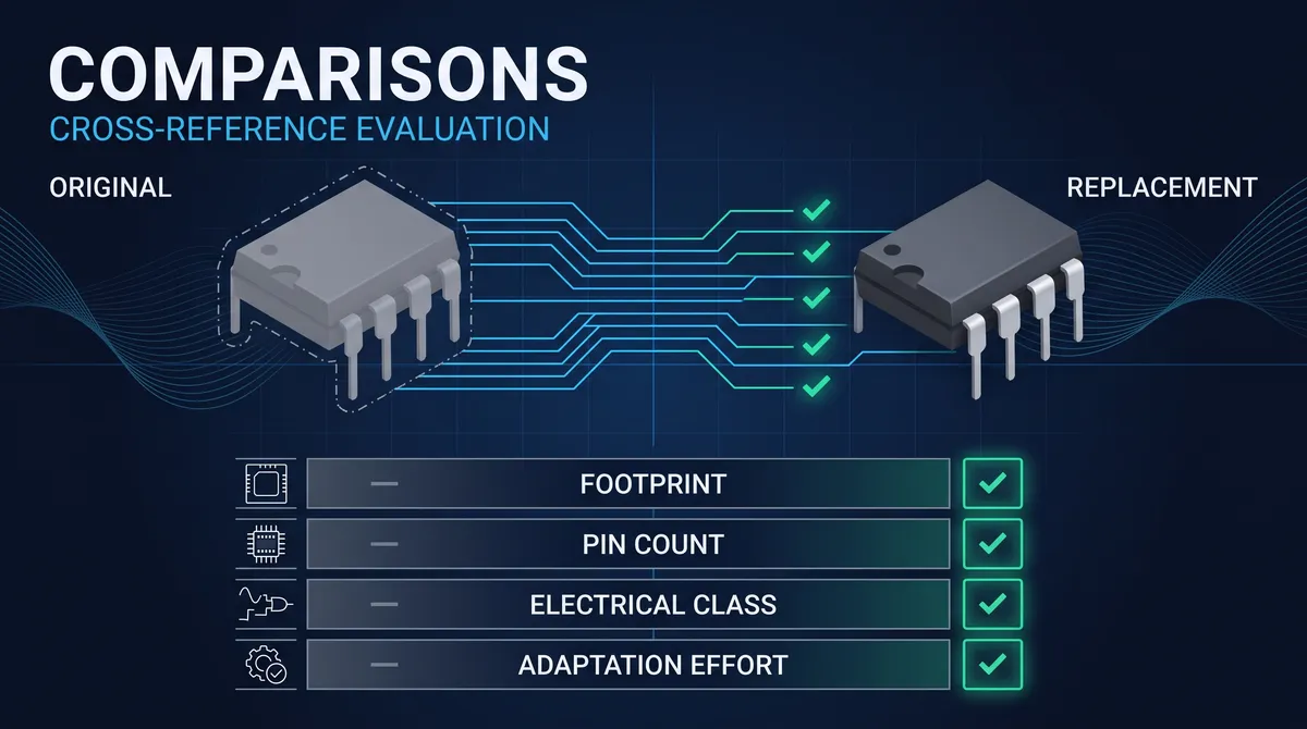
Package type and footprint verification ensures physical interchangeability between original and replacement devices. The 74HC245 is commonly available in SOIC-20, TSSOP-20, and DIP-20 packages, with footprint dimensions varying between surface-mount options. The SN74HC245 and competing alternatives typically maintain footprint compatibility within manufacturing tolerances, but dimensional verification against original PCB land pattern dimensions remains advisable. Pin spacing, lead width, and overall body dimensions should be confirmed through manufacturer datasheet comparison. Any differences in package height may affect enclosure fit or heat sink clearance.
Pinout mapping verification confirms that all signal, power, and ground connections match between original and replacement devices. The standard 74HC245 pinout described earlier should be verified for the specific replacement candidate, as some vendors may offer variant pinouts optimized for particular applications. Direction control and output enable polarity should be confirmed, particularly for parts from manufacturers serving markets with different convention preferences. Pin names and numbers should be cross-referenced between datasheets to identify any subtle differences in pin assignments that could cause functional failures.
Electrical parameter comparison against application requirements determines whether the replacement device provides adequate margin for the specific operating conditions. Key parameters requiring comparison include supply voltage range, input voltage thresholds, output drive capability, propagation delay, and power consumption. The application-specific stress factors including operating temperature, switching frequency, load capacitance, and bus termination should be evaluated against datasheet specifications to verify adequate design margin. Parameters with marginal or negative margin require either de
Timing compatibility verification ensures that replacement device propagation delays and edge rates meet system timing requirements for address, data, and control signal paths. Setup and hold time requirements for downstream logic elements must be satisfied with replacement device delays substituted for original delays. The effect of increased propagation delay on maximum operating frequency should be calculated to verify that system performance requirements remain achievable. Enable and disable times affect bus arbitration timing and should be verified against system bus protocol specifications.
ESD and latch-up protection verification confirms that replacement devices provide adequate robustness for the application environment. The SN74HC245 specifies ESD protection levels that meet or exceed typical application requirements, but generic alternatives may specify lower protection levels or omit protection specifications entirely. Latch-up immunity testing, while not always specified on datasheets, represents an important consideration for applications exposed to transients or radiation environments. Manufacturer quality certifications and reliability data should be reviewed to confirm adequate protection characteristics.
Manufacturing and assembly compatibility verification addresses concerns related to solderability, moisture sensitivity, and thermal stress during production. The SN74HC245 specifies MSL (Moisture Sensitivity Level) 1, indicating unlimited floor life at standard factory conditions, while some alternative sources may specify lower MSL ratings requiring additional handling precautions. Lead-free solder compatibility and peak reflow temperature ratings should be verified against production assembly processes. Package warpage specifications for large-body packages such as TSSOP-20 may affect yield in reflow assembly processes.
Troubleshooting Common Replacement Issues
Despite careful verification, replacement of the 74HC245 with an alternative device may encounter issues that manifest during prototype testing, production validation, or field deployment. Understanding common failure modes and their root causes enables rapid diagnosis and resolution, minimizing schedule impact when component substitutions become necessary.
Intermittent logic failures during temperature cycling often indicate marginal timing margin that becomes insufficient at temperature extremes. The original 74HC245 may have exhibited timing behavior near the specification maximum at room temperature, with replacement devices showing worse-case delays at high temperature that violate setup or hold requirements. Solution approaches include reducing operating frequency to increase timing margin, adding wait states to the bus protocol to accommodate slower edge rates, or selecting a replacement with tighter propagation delay specifications. Temperature cha
Excessive ground bounce or VCC sag during simultaneous switching represents another common issue when replacement devices exhibit faster edge rates or higher peak transient currents than the original. The SN74HC245 typically provides controlled output edge rates that minimize EMI and transient effects, but some alternative sources may specify faster edges that increase di/dt demands on the supply distribution network. Solution approaches include adding series termination resistors to slow edges, improving PCB decoupling with additional capacitance, or selecting a replacement with specified maximum edge rate limits.
Output voltage level marginality can cause compatibility issues with downstream logic, particularly when mixing HC-family devices with HCT or TTL inputs. The replacement 74HC245 output VOH may be marginally below the required VIH of following stages, creating a condition where logic appears to function at room temperature but fails when temperature, supply voltage, or loading conditions vary. Oscilloscope verification of actual output voltage levels under worst-case conditions confirms whether level marginality exists. Adding weak pull-up resistors or selecting a replacement with stronger output drive may resolve marginality issues.
High-frequency oscillation or RFI emission problems may occur when replacement devices exhibit higher-frequency resonance characteristics than the original. The output stage's interaction with load capacitance and trace inductance can create LC resonant circuits that ring at frequencies above the device's intended operating range, generating broadband noise that interferes with radio receivers or other sensitive circuits. Solution approaches include adding series damping resistors, improving shielding, or selecting a replacement with specified maximum output transition times.
Latch-up or catastrophic failure during power-up or transient events indicates insufficient protection against voltage or current stress. Replacement devices from unverified sources may lack adequate input clamping diodes, output protection structures, or process-level latch-up immunity. Oscilloscope capture of supply voltage and output waveforms during power-up sequences often reveals the transient conditions causing failure. Implementing external protection circuits or selecting a replacement with guaranteed latch-up immunity specifications resolves these issues.
Making the Final Selection: Decision Framework
The selection between the SN74HC245 and alternative 74HC245 replacements ultimately requires balancing multiple factors including technical requirements, cost constraints, supply chain considerations, and quality objectives. No single answer satisfies all application contexts, making a systematic decision framework essential for consistent, defensible selection outcomes across engineering projects.
Technical requirement mapping provides the foundation for selection decisions by establishing the minimum acceptable specifications that any replacement must satisfy. This mapping should identify non-negotiable parameters such as supply voltage range, temperature grade, package type, and timing requirements, along with desirable but flexible parameters such as propagation delay maximum, drive strength, and ESD rating. The SN74HC245 datasheet should be compared against this requirement map to confirm compliance across all non-negotiable parameters. Generic alternatives require more extensive verification to confirm compliance, potentially requiring sample testing or characterization.
Cost analysis should include not only unit price but also total cost of ownership factors that affect production economics. Unit price differences between SN74HC245 and generic alternatives may appear significant in isolation but represent a small fraction of total product cost for most applications. Quality-related costs including inspection, testing, and potential field failure should be estimated and added to unit price for meaningful comparison. Supply continuity value, representing the expected cost of production interruption if preferred sources become unavailable, should be estimated based on production volumes and market conditions.
Supplier evaluation considers factors beyond component specifications that affect long-term procurement success. Authorized distribution availability ensures access to factory-fresh stock with proper handling and traceability. Manufacturer technical support quality affects ability to resolve application issues during development and production. Quality system certifications including ISO 9001, IATF 16949 (automotive), and AS9100 (aerospace) indicate manufacturing process discipline that correlates with component reliability. Financial stability of suppliers affects long-term availability and support continuity.
Risk assessment quantifies the probability and impact of various failure scenarios associated with each selection option. Supply disruption risk considers market conditions, manufacturer capacity, and component lifecycle status. Quality risk considers historical field failure rates, process capability indices, and verification test coverage. Substitution risk considers the engineering effort required if a preferred source becomes unavailable in the future. These risks should be weighted according to application severity and customer requirements before finalizing the selection decision.
The 74HC245 replacement alternative selection should ultimately optimize for the specific application context while maintaining appropriate engineering conservatism. For safety-critical automotive and medical applications, the SN74HC245-Q1 or equivalent from established automotive-qualified suppliers provides the highest confidence in quality and reliability. For industrial applications with extended lifecycle requirements, SN74HC245 with industrial temperature grade offers good balance of specification compliance and supply chain stability. For consumer applications with cost pressure and shorter product lifecycles, generic 74HC245 alternatives may provide acceptable quality at reduced cost, provided adequate verification testing confirms compliance with application requirements.
This comprehensive comparison between the 74HC245 and SN74HC245 demonstrates that while both devices offer fundamentally identical functionality and pinout configurations, meaningful differences exist in specification characterization, quality grades, and supply chain characteristics. The SN74HC245 provides enhanced specification confidence, broader temperature grade options, and documented quality certifications that support demanding applications, while generic alternatives may offer cost advantages for less critical deployments. Selection decisions should flow from systematic requirements analysis, ensuring that chosen replacement alternatives provide adequate margin and reliability for their intended applications while respecting cost and procurement constraints.
Not sure which sensor fits your project?
Talk to our mmWave application engineers for a free consultation.
Specify your hotel project with our engineers
Send your room count, ceiling type, and protocol preference. We will return a sample plan and quote within 24 business hours.
- Move from general guidance into a product or application discussion.
- Use RFQ when pricing, drawings, MOQ, or launch timing needs structure.
- Keep a direct contact path visible for fast clarifications and handoff.