HT7333 Low Dropout Regulator: Pin-to-Pin Replacement and Cross Reference Guide
Comprehensive guide to HT7333 LDO regulator pin-to-pin replacements, cross-reference alternatives, specifications, and selection criteria for engineering procurement.
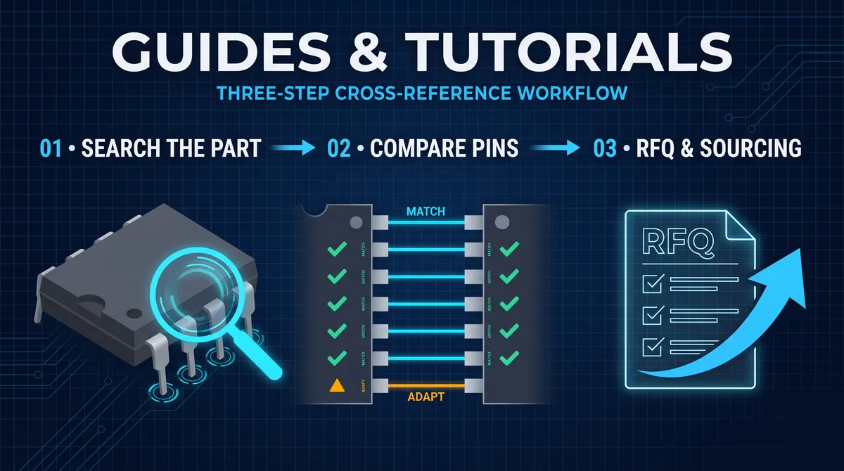
HT7333 Low Dropout Regulator: Pin-to-Pin Replacement and Cross Reference Guide
Introduction to the HT7333 LDO Regulator Family
The HT7333 represents a widely adopted low dropout linear voltage regulator family that delivers a fixed 3.3V output from input voltages as low as 3.4V, making it essential for battery-powered applications, sensor interfaces, and microcontroller power rails in industrial automation, consumer electronics, and IoT device architectures. These regulators typically provide up to 250-300mA of continuous output current while maintaining a low quiescent current of approximately 4-8µA, which is critical for extending battery life in portable and remotely deployed equipment. The HT7333 family achieves dropout voltages of 100-400mV depending on load current, enabling efficient operation even when input voltage headroom is severely limited. Engineers frequently seek an HT7333 regulator replacement alternative when sourcing constraints arise, when enhanced thermal performance is required, or when specific automotive or industrial certifications necessitate a qualified substitute component. The regulator's compact SOT-89, SOT-23-5, and TO-92 package options have made it a staple in space-constrained designs, while its wide input voltage range of 3.4V to 12V provides flexibility across multiple power bus architectures. This guide examines the HT7333's electrical characteristics, pin configurations, and comprehensive cross-reference options that maintain pin-to-pin compatibility while offering differentiated performance characteristics for specialized applications.
The HT7333 regulator family operates through a series-pass transistor architecture that regulates output voltage by comparing a reference voltage against a divided version of the output through an internal error amplifier, achieving typical line regulation of 0.05%/V and load regulation of 0.01%/mA in well-designed implementations. The regulator's thermal shutdown activates at junction temperatures exceeding 150°C, protecting against catastrophic failure during output short-circuit conditions or excessive power dissipation events. Built-in current limiting circuitry typically clamps output current at 300-500mA during fault conditions, providing a balance between load protection and inrush current allowance for capacitive loads. The devices integrate a reverse-battery protection diode that prevents damage when input voltage is applied in reverse polarity, a feature particularly valuable in automotive and industrial environments where wiring errors can occur during installation or maintenance. Power supply rejection ratio (PSRR) typically measures 65-70dB at 1kHz, sufficient for filtering moderate switching noise from upstream power sources but potentially requiring additional filtering for extremely noise-sensitive analog circuits. Understanding these fundamental characteristics enables engineers to properly evaluate HT7333 regulator replacement alternative options that maintain equivalent protection features while addressing specific application constraints such as extended temperature range, reduced dropout, or enhanced ESD robustness.
Technical Specifications and Electrical Parameters
The HT7333 family specifications define a precise operating envelope that engineers must match when selecting cross-reference alternatives for their specific application requirements and environmental conditions. Input voltage range spans from 3.4V minimum to 12V maximum for standard commercial grades, with some manufacturer variants supporting extended ranges up to 15V or 18V for industrial bus compatibility, and automotive-grade versions typically limited to 6V or 8V maximum while offering improved temperature and ruggedization performance. Output voltage tolerance at room temperature typically holds within ±2% for standard commercial grades, with precision variants available offering ±1% or tighter tolerance for applications requiring accurate reference voltages such as battery charging circuits or sensor excitation supplies. Output voltage temperature coefficient commonly ranges from ±50ppm/°C to ±100ppm/°C depending on the specific manufacturing process and voltage reference architecture employed within the device.
The HT7333 regulator replacement alternative selection process requires careful attention to output current capability, dropout voltage performance, and thermal resistance characteristics to ensure reliable long-term operation in the target application environment. Continuous output current ratings typically specify 250mA or 300mA depending on package type and manufacturer, with thermal considerations often limiting usable current at elevated ambient temperatures due to package-to-ambient thermal resistance constraints. Dropout voltage at 100mA load current typically measures 100-150mV for standard HT7333 variants, increasing to 250-400mV at maximum rated current, which directly impacts minimum input-to-output voltage differential required for proper regulation. Quiescent current consumption of 4-8µA under no-load conditions represents a critical specification for battery-powered applications, as this current flows continuously regardless of load state and directly affects standby power consumption and battery shelf life. Standby current when the device enters shutdown mode typically reduces to 0.1µA or less, enabling significant power savings in microcontroller-based systems that periodically enable and disable power rails to manage overall system energy budget.
| Parameter | HT7333-3.3 Standard | HT7333-3.3 Precision | Typical Units |
|---|---|---|---|
| Output Voltage | 3.3 | 3.3 | V |
| Output Tolerance (25°C) | ±2% | ±1% | - |
| Output Voltage Temp Coeff. | 50-100 | 25-50 | ppm/°C |
| Input Voltage Range | 3.4 - 12 | 3.4 - 12 | V |
| Dropout Voltage (100mA) | 100-150 | 100-150 | mV |
| Dropout Voltage (250mA) | 300-400 | 300-400 | mV |
| Max Output Current | 250-300 | 250-300 | mA |
| Quiescent Current (no load) | 4-8 | 4-8 | µA |
| Quiescent Current (shutdown) | <0.1 | <0.1 | µA |
| PSRR @ 1kHz | 65-70 | 65-70 | dB |
| Output Noise Voltage | 30-50 | 20-30 | µVrms |
| Short-Circuit Current Limit | 300-500 | 300-500 | mA |
| Thermal Shutdown Temp | 150-160 | 150-160 | °C |
Thermal management considerations become increasingly important when evaluating HT7333 regulator replacement alternative options, as the combined effect of ambient temperature, thermal resistance from junction to ambient, and power dissipation determines safe operating area limits. Power dissipation calculates as the product of output current and input-to-output voltage differential, with a practical example being 100mA × (5V - 3.3V) = 170mW for a typical 5V to 3.3V conversion at room temperature. The SOT-89 package typically offers junction-to-ambient thermal resistance of 120-150°C/W without external heatsinking, which limits maximum power dissipation to approximately 500mW at 70°C ambient temperature, yielding a maximum output current capability of roughly 150mA under these conditions. Engineers must verify that any HT7333 regulator replacement alternative provides thermal performance equal to or better than the original component, particularly in sealed enclosures or high-ambient-temperature industrial environments where thermal margins may already be compressed.
Pin Configuration and Package Compatibility
The HT7333 family appears in multiple package options, with the SOT-89 three-pin configuration serving as the industry-standard footprint that enables straightforward pin-to-pin replacement using alternative parts from different manufacturers. The SOT-89 package assigns the input voltage (VIN) to pin 1, ground (GND) to pin 2, and output voltage (VOUT) to pin 3, with the exposed pad (if present) typically connected to the ground plane for enhanced thermal performance. This three-terminal configuration mirrors the pinout of numerous competing LDO regulators including the AMS1117-3.3, LM317-3.3 equivalent, and various manufacturer-specific 3.3V LDO families, creating broad compatibility for drop-in replacement scenarios. The SOT-23-5 variant adds an enable/shutdown control pin and potentially a reference bypass pin, enabling lower-power modes and improved noise performance at the cost of requiring additional circuit board routing and control signal management. The TO-92 through-hole package option provides a familiar form factor for hobbyist and educational applications, though its thermal performance limits output current capability compared to surface-mount alternatives.
Pin 1 of the HT7333 accepts the unregulated input voltage and connects internally to the drain of the series-pass P-channel MOSFET transistor that controls the output voltage by varying its on-resistance in response to the error amplifier output. This input pin should be bypassing with a minimum of 1µF to 10µF tantalum or ceramic capacitor positioned close to the device to ensure stability and transient response performance, with larger capacitance values providing improved input filtering for noisy power sources. Pin 2 provides the ground reference for both the internal circuit operation and the output voltage measurement, requiring a low-impedance connection to the system ground plane to maintain accurate regulation and minimize ground-loop errors in sensitive analog applications. Pin 3 delivers the regulated output voltage to the load, with the recommended output capacitor of 1µF to 22µF required for stability as specified in the manufacturer's datasheet, as LDO regulators with inadequate output capacitance can exhibit oscillation or degraded transient response.
When selecting an HT7333 regulator replacement alternative, engineers must verify exact pinout compatibility including the orientation of the three standard pins and the presence of any additional pins in multi-pin packages that may require different board-level routing. The SOT-89 package physical dimensions and pin spacing must match the original footprint to ensure proper solder joint formation and mechanical alignment during assembly or rework operations. Some third-party manufacturers produce extended-temperature or automotive-qualified alternatives that use identical SOT-89 packages but require higher-quality PCB layout practices such as thermal vias and ground plane extensions to achieve rated performance in demanding environments. Package height variations exist between manufacturers, with typical SOT-89 heights ranging from 1.2mm to 1.5mm, which rarely impacts most applications but should be verified for extremely space-constrained assemblies or when stacking multiple boards in compact enclosures.
Cross-Reference Alternatives: Pin-Compatible Options
The market offers numerous pin-compatible alternatives to the HT7333 regulator, each providing specific performance improvements or certifications that may benefit particular application categories while maintaining the essential three-terminal SOT-89 footprint. The AMS1117-3.3 from Advanced Monolithic Systems provides a widely available alternative with similar 3.3V output and 1A rated current capability, though its higher dropout voltage of approximately 1.2V and quiescent current of 5-10mA make it more suitable for applications where input voltage headroom is plentiful and power consumption is less critical. The MCP1700 from Microchip offers an excellent HT7333 regulator replacement alternative with ultra-low quiescent current of 1.6µA typical, 250mA output current, and only 178mV dropout at 250mA, making it ideal for extremely power-sensitive battery applications where the original HT7333's consumption is unacceptable. The TPS73601 from Texas Instruments provides a different twist with its error-reference bypass pin enabling ultra-low noise performance of 30µVrms while maintaining 400mA output capability and low dropout performance.
The AP2112 from Diodes Incorporated represents another strong pin-compatible option offering 3.3V output at 600mA with a dropout of approximately 250mV at full load, plus an enable pin for power sequencing control in multi-rail systems. The RT9166 from Richtek delivers low dropout performance of 150mV at 300mA with excellent line and load regulation specifications suitable for demanding industrial control applications. For automotive applications requiring extended temperature range and enhanced reliability, the NCV8710 from ON Semiconductor provides AEC-Q100 qualification with operation from -40°C to 125°C junction temperature, making it an appropriate HT7333 regulator replacement alternative for automotive electronics modules. The MIC5225 from Microchip offers a combination of low quiescent current at 30µA, 150mV dropout at 150mA, and integrated thermal shutdown and current limiting protection in a SOT-23-5 package with enable control.
| Part Number | Manufacturer | Output Voltage | Max Current | Dropout @ 100mA | Iq (typ) | Package | Qualification |
|---|---|---|---|---|---|---|---|
| HT7333 | Holtek/UTC | 3.3V | 300mA | 100mV | 4µA | SOT-89 | Commercial |
| MCP1700 | Microchip | 3.3V | 250mA | 178mV | 1.6µA | SOT-89 | Commercial/Automotive |
| AMS1117-3.3 | AMS | 3.3V | 1000mA | 1000mV | 5000µA | SOT-89 | Commercial |
| TPS73601 | TI | 3.3V | 400mA | 75mV | 120µA | SOT-89 | Commercial |
| AP2112 | Diodes | 3.3V | 600mA | 250mV | 55µA | SOT-89 | Commercial |
| RT9166 | Richtek | 3.3V | 300mA | 150mV | 80µA | SOT-89 | Commercial |
| NCV8710 | ON Semi | 3.3V | 150mA | 170mV | 9µA | SOT-89 | AEC-Q100 |
| MIC5225 | Microchip | 3.3V | 150mA | 150mV | 30µA | SOT-23-5 | Commercial |
The NCP4620 from ON Semiconductor provides an interesting HT7333 regulator replacement alternative with high input voltage capability up to 16V, enabling use in 12V automotive and industrial systems without additional protection circuitry. Its 150mA output current and 400mV dropout at rated current position it as a middle-ground option between the low-power HT7333 and higher-current alternatives. The BL8064 from Bestechnic offers another perspective with its 300mA output, 12V input capability, and low quiescent current of 2.5µA, achieving an excellent balance between power efficiency and flexibility in embedded systems designs. Engineers should note that while these alternatives maintain pin compatibility, minor differences in recommended external components, particularly output capacitor specifications, may require board-level adjustments to ensure optimal performance and stability.
Selection Criteria for HT7333 Replacement Alternatives
Choosing the appropriate HT7333 regulator replacement alternative requires systematic evaluation of multiple technical parameters matched against specific application requirements and environmental constraints. The minimum input voltage specification must satisfy the relationship VIN(min) = VOUT + VDO(max) + margin, where VDO(max) represents the maximum dropout voltage at expected load current and operating temperature, and the margin accounts for input voltage ripple and transients that could otherwise cause momentary loss of regulation. Applications powered from 4.2V lithium-ion batteries with 3.3V loads require regulators capable of operation below 3.4V input due to battery discharge curves, necessitating alternatives with dropout voltages below 100mV to maintain regulation throughout the battery discharge cycle. In contrast, applications with regulated 5V or 9V input rails have abundant headroom, allowing selection of alternatives that trade off dropout performance for other desirable characteristics such as lower noise, higher output current, or reduced quiescent current.
Thermal performance evaluation involves calculating the expected power dissipation using worst-case conditions including maximum load current, minimum input voltage, and maximum ambient temperature, then comparing this value against the thermal resistance from junction to ambient for the selected package. The junction temperature estimate of TJ = TA + (PD × θJA) must remain below the maximum rated junction temperature, typically 125°C for commercial grades or 150°C for industrial grades, with adequate margin for temperature measurement uncertainty and component degradation over operating life. For applications requiring operation above 70°C ambient temperature, engineers should specifically seek HT7333 regulator replacement alternative options with lower thermal resistance or higher maximum junction temperature ratings, or consider alternative packages such as DFN or QFN that offer improved thermal performance through exposed pad connectivity to the PCB ground plane.
The enable/shutdown functionality becomes critical in system-level designs where dynamic power management enables selective enabling of power rails to conserve energy during low-activity periods or implement controlled power-up sequences that prevent brownout conditions. If the original HT7333 application uses only the three standard pins without enable functionality, adding an alternative with enable requires either adding external control circuitry or selecting an alternative that defaults to enabled state when the enable pin is floating. Some regulators implement active-high enable logic while others use active-low enable, requiring attention to the control signal polarity when integrating shutdown control into existing designs. The output capacitor specification also warrants careful review, as some alternatives require minimum ESR within a specific range for stability, while others accept a wider range of capacitor types including lower-ESR ceramic capacitors that may be preferred for space or cost reasons.
Application Circuit Design Guidelines
Implementing a reliable HT7333 regulator replacement alternative circuit requires attention to input filtering, output bypassing, and PCB layout practices that ensure stable regulation under all load conditions. The input capacitor serves multiple functions including providing transient current during load steps when the regulator cannot immediately respond, filtering high-frequency noise from the input supply, and establishing a local charge reservoir that reduces voltage sag during rapid load current demands. A minimum 1µF ceramic capacitor positioned within 2mm of the input pin provides adequate performance for most applications, with larger values of 4.7µF to 10µF recommended when the input source impedance is high or when load transients exceed 50mA. When the input supply is located more than a few centimeters from the regulator, additional bulk capacitance of 10µF to 47µF at the point of entry helps prevent voltage overshoot and ringing on the supply lines.
The output capacitor requirement for LDO stability typically specifies a minimum capacitance and maximum ESR range that must be satisfied to prevent oscillation or degraded transient response. Standard HT7333-compatible regulators require 1µF minimum output capacitance with ESR between 10mΩ and 500mΩ, a range that comfortably accommodates ceramic, tantalum, and electrolytic capacitor technologies. Using low-ESR ceramic capacitors directly on the output provides excellent transient response but may require attention to dc bias effects that reduce effective capacitance at rated voltage, particularly for small case size capacitors such as 0402 or 0603. Larger case sizes such as 0805 or 1206 maintain more consistent capacitance under bias conditions. Adding a small series resistance of 1-5Ω between the regulator output and purely capacitive loads can improve stability when using low-ESR ceramic capacitors, though this resistance reduces effective load voltage under current flow and should be included in the overall voltage budget calculations.
For noise-sensitive applications such as RF power amplifiers, sensor excitation, or precision analog-to-digital converter references, additional output filtering may be required beyond what the basic LDO provides. Adding a passive LC filter comprising a 10µH inductor and 10µF capacitor between the regulator output and sensitive load circuitry provides approximately 40dB of additional high-frequency attenuation at the cost of increased voltage drop and reduced load transient response speed. Alternatively, selecting an HT7333 regulator replacement alternative with built-in noise reduction features such as reference bypass pins or ultra-low-noise architectures can achieve similar results without additional component count. The TPS73601 mentioned earlier exemplifies this approach, achieving output noise below 30µVrms through its innovative architecture that eliminates the noise contribution of the bandgap reference. For applications requiring sub-microvolt noise floors, consider dedicated low-noise regulators such as the LT3042 from Analog Devices or similar precision architectures designed specifically for instrumentation applications.
Thermal Management Strategies
Effective thermal management ensures reliable long-term operation of the HT7333 and its replacement alternatives by maintaining junction temperatures within rated limits under all specified operating conditions. The relationship between power dissipation, thermal resistance, and temperature rise follows the familiar equation ΔT = PD × θ, where power dissipation equals the product of output current and input-output voltage differential. For a 5V input, 3.3V output, 100mA load scenario, power dissipation calculates to 170mW, which produces a temperature rise of approximately 20-25°C above ambient when using a standard SOT-89 package with θJA of 120-150°C/W. This leaves comfortable margin for 70°C ambient operation, but the situation changes dramatically when input voltage increases or load current rises. At 12V input with 250mA load, power dissipation reaches 2.175W, exceeding the safe dissipation capability of a standard SOT-89 package and necessitating either a better-thermal package option, external heatsinking, or reduced load current specification.
PCB layout significantly impacts thermal performance by providing a heat spreading path from the regulator package to the surrounding ambient air and system enclosure. The thermal vias connecting the exposed pad to internal ground planes should use thermal relief spokes rather than solid connections to balance mechanical reliability during thermal cycling with thermal conductivity requirements. Multiple thermal vias of 0.3mm to 0.4mm diameter provide adequate heat transfer without compromising PCB manufacturing yield or introducing excessive plating voids. Surrounding the regulator footprint with a solid copper ground plane extending at least 5mm beyond the package boundaries dramatically improves heat spreading compared to narrow trace connections. In extreme thermal environments or when operating near maximum rated power, consider using thicker copper weight of 2oz or 3oz PCB material to further enhance thermal conductivity and reduce temperature rise.
Alternative packages from the same manufacturer or third-party alternatives often provide improved thermal options that accept HT7333 regulator replacement alternative strategies for thermally challenging applications. The SOT-223 package offers approximately three times the thermal performance of SOT-89 due to its larger body and exposed pad area, though it requires different PCB footprint and may not be directly compatible with boards designed for SOT-89 packages. The DFN/QFN packages with bottom-side thermal pads provide excellent thermal performance when properly soldered to the PCB, achieving θJA values below 60°C/W in some configurations, but require careful inspection to verify solder joint integrity. For applications where PCB modifications are impractical, external heatsinking using clip-mounted or adhesive-backed heatsink solutions can extend the thermal capability of existing SOT-89 packages, though the mechanical attachment reliability should be evaluated for environments subject to vibration or thermal cycling.
Automotive and Industrial Application Considerations
Automotive applications impose stringent requirements on electronic components that the standard commercial-grade HT7333 cannot satisfy, driving engineers to seek HT7333 regulator replacement alternative options with appropriate automotive qualifications and extended environmental specifications. The AEC-Q100 standard defines a comprehensive qualification sequence including accelerated life testing, electrostatic discharge sensitivity testing, and temperature cycling that ensures component reliability in the demanding automotive environment. Automotive regulators must typically operate across the full -40°C to 125°C junction temperature range while withstanding battery transient conditions including reverse battery, load dump, and jump-start scenarios that can subject the input circuit to voltages exceeding 24V for brief periods. The NCV8710 and similar automotive-qualified regulators incorporate input transient protection that clamps overvoltage conditions and prevents damage during these extreme events.
Industrial applications present different challenges than automotive environments, with primary concerns centering on extended operating temperature ranges, long-term availability guarantees, and enhanced reliability under continuous operation conditions. Industrial-grade regulators typically specify operation from -40°C to 85°C ambient or junction temperatures, with some versions extending to 105°C or 125°C for equipment deployed in unventilated enclosures or near heat-generating components. The extended temperature range directly impacts quiescent current specifications, as semiconductor leakage currents increase exponentially with temperature, potentially tripling or quadrupling the room-temperature consumption at elevated temperatures. For battery-powered industrial sensors and wireless monitoring nodes deployed in locations with limited maintenance access, selecting an HT7333 regulator replacement alternative with minimal elevated-temperature quiescent current directly extends battery service life and reduces maintenance frequency.
Electromagnetic compatibility (EMC) considerations influence regulator selection for applications where the LDO must operate in electrically noisy environments such as motor drives, switching power supplies, or radio transceivers. The power supply rejection ratio (PSRR) specification quantifies the regulator's ability to attenuate input voltage ripple, with higher PSRR values indicating better filtering of upstream noise. Standard HT7333 devices typically provide 65-70dB PSRR at 1kHz, adequate for filtering moderate switching noise but potentially insufficient for applications with high-frequency switching regulators or strong RF interference coupling. Some LDO alternatives feature enhanced PSRR architectures achieving 80dB or higher at 1kHz, though this often comes at the expense of higher quiescent current or reduced output current capability. For applications with severe EMC requirements, consider combining a standard regulator with external LC filtering or selecting a regulator specifically optimized for high-frequency PSRR performance.
Procurement and Supply Chain Management
Sourcing reliable HT7333 regulator replacement alternatives requires attention to distributor availability, manufacturer support, and long-term supply chain stability that ensures component availability throughout the product lifecycle. The original HT7333 is manufactured by multiple companies including Holtek Semiconductor and UTC, with varying levels of quality consistency and technical support that sometimes necessitate qualification of alternative sources. When qualifying replacement alternatives, obtain samples from multiple distributors and test across several date codes to verify consistent performance before committing to production volumes. Distributors such as Digi-Key, Mouser, Arrow, and Avnet maintain broad inventory of popular LDO alternatives, though specialized or automotive-qualified variants may require ordering through franchise distribution channels with longer lead times.
Part number standardization across manufacturers simplifies procurement and reduces the risk of counterfeit components entering the supply chain, as cross-referenced parts with identical markings may have originated from different fabs with potentially different process technology or quality controls. Requesting lot traceability documentation and certificates of analysis helps verify component authenticity and manufacturing origin, particularly for safety-critical applications where regulator failure could result in system-level hazards. Some procurement teams maintain qualified alternate source (QAS) lists that pre-approve specific HT7333 regulator replacement alternative options for various application categories, enabling rapid substitution when primary sources experience allocation or discontinuation without requiring full requalification. Establishing these relationships before supply disruptions occur provides supply chain resilience that reduces production delays and excess inventory risk.
Pricing considerations vary significantly across the HT7333 family and its alternatives, with commercial-grade standard variants available for under $0.05 per unit in high volume while automotive-qualified or precision-grade alternatives may cost $0.20 to $0.50 each depending on manufacturer and qualification level. Unit cost differences rarely dominate total system cost in applications where the regulator represents a small fraction of overall bill of materials, but they become relevant in high-volume consumer products or cost-sensitive industrial equipment where even $0.01 differences compound across millions of units. Engineers should balance unit cost against total cost of ownership including inventory carrying costs, qualification expenses, and potential field failure costs that might result from using inadequately qualified alternatives. For long-lifecycle industrial or infrastructure applications, consider the availability risk of niche alternatives that might be discontinued before the end of the product's service life, potentially requiring another qualification cycle and associated engineering expense.
Quality and Reliability Verification
Verifying that an HT7333 regulator replacement alternative meets quality and reliability requirements involves a combination of datasheet review, sample testing, and sometimes extended qualification depending on the application's criticality and expected operating environment. The datasheet specification review should confirm that all critical parameters exceed the original component's ratings with appropriate margin, typically requiring replacement alternatives to match or improve upon the HT7333's specifications by at least 10-20% in key areas. Parameters requiring particular attention include dropout voltage at expected load current, quiescent current across the full temperature range, output voltage tolerance including temperature effects, and short-circuit/overcurrent protection levels. Subtle differences in protection circuitry implementation may result in different behavior during abnormal operating conditions that affect system-level reliability in edge cases.
Accelerated life testing under elevated temperature and voltage conditions helps identify potential failure modes that might not manifest during short-term functional testing but could affect long-term reliability in the field. A simplified qualification sequence might include 168 hours of high-temperature operating life testing at maximum rated temperature and voltage, followed by temperature cycling between hot and cold extremes to identify package or die attach issues, and conclude with biased humidity testing for applications subject to moisture exposure. For consumer applications with limited warranty exposure, this abbreviated qualification may provide sufficient confidence, while safety-critical applications such as medical devices, automotive systems, or aerospace equipment require more comprehensive qualification following industry-specific standards and extended testing durations.
Statistical process control and outgoing quality level (OQL) agreements with distributors provide additional assurance that replacement alternatives continue to meet specifications over time as manufacturing processes evolve and mature. Requesting screening data for critical parameters such as output voltage, dropout voltage, and quiescent current helps identify lot-to-lot variation that might affect system performance or interoperability with other components sharing the same power rail. Some manufacturers offer automotive or industrial grade variants with enhanced screening and documentation that simplifies system-level qualification, potentially making these higher-priced alternatives more cost-effective when accounting for reduced engineering qualification effort. Establishing incoming inspection protocols that verify key parameters on samples from each lot provides early detection of any supply chain issues that might result in out-of-specification components reaching the production line.
Conclusion and Summary
The HT7333 low dropout regulator family serves as a fundamental building block in countless electronic systems, but sourcing constraints, enhanced performance requirements, or application-specific qualifications frequently necessitate identifying appropriate HT7333 regulator replacement alternative options that maintain pin-to-pin compatibility while delivering differentiated capabilities. The comprehensive cross-reference analysis presented in this guide identifies numerous pin-compatible alternatives ranging from ultra-low-power options like the MCP1700 with 1.6µA quiescent current to high-current solutions like the AP2112 with 600mA capability, and from standard commercial grades to fully automotive-qualified devices suitable for safety-critical applications. Selection of the optimal replacement requires careful evaluation of input voltage range, output current requirements, dropout performance, quiescent current consumption, thermal management considerations, and any application-specific qualification requirements that affect long-term reliability.
The technical specifications, pin configuration details, and application guidance provided throughout this article equip engineers with the foundational knowledge required to evaluate replacement options confidently and implement successful substitutions in both prototype and production environments. Thermal management strategies enable reliable operation across expanded temperature ranges, while automotive and industrial application considerations highlight the specialized requirements that drive qualification of alternative components for demanding environments. Procurement and supply chain management practices ensure continuity of supply and protection against counterfeits, and quality verification procedures validate that selected alternatives perform reliably throughout the product lifecycle. By applying these systematic evaluation criteria and leveraging the comprehensive cross-reference data, engineers can identify optimal HT7333 regulator replacement alternative solutions that satisfy both immediate substitution needs and long-term application requirements.
Not sure which sensor fits your project?
Talk to our mmWave application engineers for a free consultation.
Specify your hotel project with our engineers
Send your room count, ceiling type, and protocol preference. We will return a sample plan and quote within 24 business hours.
- Move from general guidance into a product or application discussion.
- Use RFQ when pricing, drawings, MOQ, or launch timing needs structure.
- Keep a direct contact path visible for fast clarifications and handoff.