SPI Flash Memory Cross Reference: W25Q vs MX25 vs GD25 Compatible IC Guide
Comprehensive cross-reference guide comparing Winbond W25Q, Macronix MX25, and GigaDevice GD25 SPI flash ICs for embedded systems design.
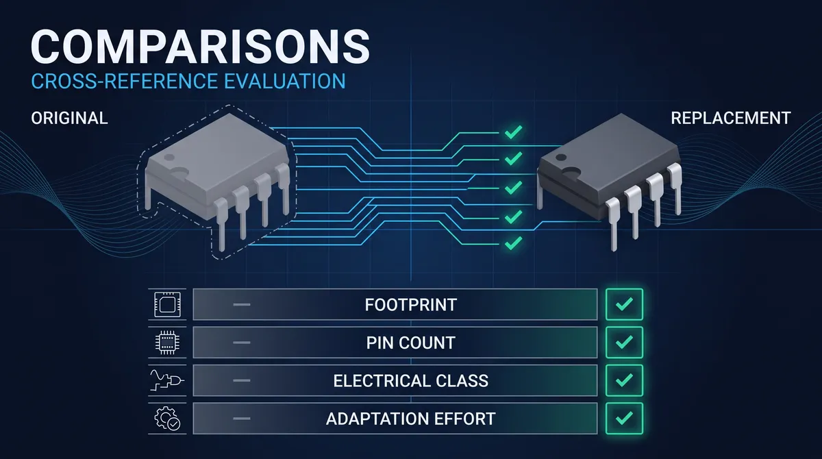
SPI Flash Memory Cross Reference: W25Q vs MX25 vs GD25 Compatible IC Guide
Introduction to SPI Flash Memory Cross-Reference Analysis
SPI flash alternative comparison has become one of the most critical decision points for embedded systems engineers, particularly when designing products that require long-term availability, cost optimization, or dual-source procurement strategies. Serial Peripheral Interface (SPI) flash memory represents the dominant non-volatile storage solution across consumer electronics, industrial automation, automotive systems, and Internet of Things (IoT) devices, with market demand exceeding 3 billion units annually. The three leading manufacturers in this space—Winbond Electronics (W25Q series), Macronix International (MX25 series), and GigaDevice Semiconductor (GD25 series)—collectively command over 75% of the global SPI flash market, yet their parts are frequently selected based on availability, pricing fluctuations, and specific application requirements rather than comprehensive technical evaluation.
This SPI flash alternative comparison guide provides an exhaustive technical cross-reference between these three major families, examining pinout compatibility, electrical specifications, performance characteristics, and real-world deployment considerations. Engineers and procurement specialists will find detailed parametric comparisons, migration strategies for design changes, and guidance on selecting the optimal SPI flash alternative for specific use cases ranging from boot storage in microcontrollers to large-capacity data logging in edge computing applications. The analysis draws on published datasheets, industry standards, and practical field experience to deliver actionable insights for both new designs and second-source qualification efforts.
Understanding the nuances of SPI flash alternative comparison requires familiarity with the underlying technology fundamentals. All three product families implement a standardized SPI interface operating at frequencies up to 133 MHz in standard mode and up to 166 MHz in quad SPI (QPI) or octal SPI modes for high-performance variants. The devices share common command protocols based on JEDEC standards, enabling software compatibility across manufacturers while maintaining device-specific optimizations. This guide examines both the technical equivalence and practical differences that engineers must consider when evaluating these SPI flash alternatives for production deployment.
Understanding SPI Flash Memory Technology and Standards
SPI flash alternative comparison begins with a solid understanding of the underlying technology architecture that enables interoperability between devices from different manufacturers. SPI flash memory utilizes a serial interface protocol originally developed by Motorola in the 1980s, adapted for flash memory operations through standardized command sets defined by the Joint Electron Device Engineering Council (JEDEC). The JEDEC JEDEC Standard No. 216A establishes the common command interface for serial flash memories, ensuring that basic read, write, and erase operations follow consistent patterns regardless of the silicon vendor.
The fundamental SPI interface consists of four signal lines: Serial Clock (SCLK), Master Out Slave In (MOSI), Master In Slave Out (MISO), and Chip Select (CS). This 4-wire interface enables simple routing on PCB layouts while maintaining sufficient bandwidth for most embedded applications. Modern SPI flash devices, including the W25Q, MX25, and GD25 families, extend this basic interface with multi-I/O modes that dramatically increase throughput without adding pins. Dual SPI mode uses both MOSI and MISO lines for bidirectional data transfer, effectively doubling the data rate. Quad SPI mode adds two additional I/O pins (WP# and HOLD#) to achieve four-bit-wide data transfers, while octal SPI variants expand to 8-bit wide interfaces for the highest performance requirements.
Power consumption characteristics represent a critical differentiation factor in SPI flash alternative comparison for battery-powered and power-sensitive applications. The W25Q series from Winbond implements an efficient power management architecture with typical active read currents of 25 mA at 104 MHz operation and standby currents as low as 1 µA. Macronix MX25 devices achieve comparable efficiency with active currents of 20 mA and standby currents of 5 µA in deep power-down mode. GigaDevice GD25 parts offer similar power profiles with typical active consumption of 30 mA and standby current of 5 µA. For applications requiring ultra-low power consumption, all three manufacturers offer specialized low-power variants with standby currents below 1 µA and extended battery life specifications.
The organization of memory array architecture varies significantly between manufacturers despite similar density offerings. Winbond W25Q devices organize memory into 4KB sectors with 64KB blocks, enabling fine-grained erase granularity that minimizes wasted capacity during frequent small writes. Macronix MX25 parts use a similar sector architecture with some variations in block sizes across different density grades. GigaDevice GD25 devices follow comparable organizational patterns but implement different protection mechanisms and security features that engineers must understand when performing SPI flash alternative comparison for security-sensitive applications.
Winbond W25Q Series: Comprehensive Technical Analysis
The Winbond W25Q series represents the market-leading SPI flash solution with the broadest range of density options, performance grades, and specialized features. This SPI flash alternative comparison section provides detailed technical analysis of the W25Q architecture, helping engineers understand the specifications and features that make this family a frequent first choice for new designs. Winbond has established itself as the volume leader in SPI flash with annual production exceeding 1.5 billion units, providing excellent supply chain stability and competitive pricing across the product lifecycle.
The W25Q product line spans densities from 512 Kbit (64 KB) to 2 Gbit (256 MB), with the most common variants in the 8 Mbit to 128 Mbit range serving mainstream embedded applications. Each density grade maintains consistent pinout and package options, enabling seamless migration between different capacity points within the same family. The base W25Q series operates at 104 MHz maximum clock frequency with standard SPI protocol, while the W25Q-D series adds dual SPI support for effective 208 MHz data rates. The high-performance W25Q-Q series implements quad SPI operation achieving 416 MHz effective bandwidth, and the newest W25Q-J variants support QPI (Quad Peripheral Interface) with command-on-8-lines for maximum throughput.
Electrical specifications for the W25Q series demonstrate consistent performance across the product range. Supply voltage operates at 2.7V to 3.6V for standard variants, with 1.65V to 2.0V low-voltage options available for mobile and power-sensitive designs. The typical sequential read operation at 104 MHz consumes approximately 25 mA, with page program (256 bytes) completing in 0.8 ms and sector erase (4 KB) requiring 30 ms. Full chip erase operations vary from 20 seconds for smaller densities to 120 seconds for 128 Mbit parts. These timing specifications prove critical for SPI flash alternative comparison when evaluating boot time performance and programming throughput requirements.
Winbond implements a sophisticated security architecture in the W25Q series that distinguishes it from competing alternatives. The device includes 256-byte Security Register with one-time-programmable (OTP) protection, Individual Block Lock capability for fine-grained write protection, and a 128-bit Unique ID for device authentication. The W25Q series also supports volatile and non-volatile configuration register options, enabling designers to optimize performance versus power consumption on-the-fly without full device erasure. These security features make the W25Q particularly suitable for applications requiring intellectual property protection, secure boot implementation, or anti-cloning measures.
Package options for W25Q devices include standard 8-pin SOIC (150/208 mil), 8-pin WSON (6x5 mm), and 16-pin SOIC for high-pin-count variants. The W25Q-JV series offers an extended temperature range of -40°C to +105°C, addressing automotive and industrial applications. All packages maintain pin-to-pin compatibility with corresponding Macronix MX25 and GigaDevice GD25 parts in standard pinouts, enabling straightforward SPI flash alternative comparison and second-source qualification without PCB redesign.
Macronix MX25 Series: Technical Capabilities and Differentiation
The Macronix MX25 series provides strong competition in the SPI flash alternative comparison landscape, offering comparable specifications with distinctive features that appeal to specific application segments. Macronix has invested heavily in embedded flash memory technology, leveraging their experience in NOR flash manufacturing to deliver reliable, high-quality SPI devices. The MX25 family maintains particular strength in automotive, industrial, and computing applications where extended temperature range and long-term reliability are paramount considerations.
Memory organization in the MX25 series follows industry-standard patterns with some manufacturer-specific optimizations. The MX25L series (standard power) and MX25R series (low power) provide complementary options for different application requirements. Densities range from 256 Kbit to 512 Mbit, with the most popular industrial grades occupying the 8 Mbit to 64 Mbit range. Sector architecture employs 4 KB minimum erase granularity with 32 KB and 64 KB block options, matching the flexibility required for diverse application profiles. The memory array architecture supports full random access addressing, enabling efficient execution-in-place (XiP) for code storage applications.
Performance specifications for the MX25 series place it in direct competition with Winbond W25Q offerings. Maximum clock frequency reaches 133 MHz for standard SPI operation, with dual I/O mode achieving effective 266 MHz throughput and quad I/O mode reaching 532 MHz. These specifications make the MX25 particularly attractive for high-performance microcontrollers and applications requiring fast boot times. The high-speed read parameter of 133 MHz with only 2 wait states represents a meaningful improvement over earlier-generation devices, and the SPI flash alternative comparison shows MX25 matching or exceeding W25Q performance in several benchmarks.
Macronix distinguishes the MX25 series through innovative reliability features and extended product longevity. The MX25R series incorporates special low-power modes with standby current of just 1 µA, making it ideal for IoT sensors, wearable devices, and other battery-powered applications. The devices implement Macronix's proprietary PFlash technology for enhanced endurance, with specified 100,000 program/erase cycles per sector and 20-year data retention at 85°C. The extended temperature variant (MX25R-EXT) operates reliably from -40°C to +105°C, meeting stringent automotive AEC-Q100 Grade 2 requirements.
The MX25 series includes sophisticated security and protection mechanisms that merit attention during SPI flash alternative comparison. The devices feature block protection with configurable protection granularity, OTP memory regions for permanent data storage, and unique identifier registers for device authentication. Macronix implements a robust hardware write-protect scheme that prevents accidental or malicious modification of critical memory regions. The security architecture supports secure boot implementations through signature verification and encrypted execution modes on compatible microcontroller platforms.
Package offerings for MX25 devices span industry-standard options including 8-pin SOP, 8-pin WSON, and 24-ball BGA packages for space-constrained designs. The MX25U series provides 1.65V to 2.0V operation for mobile applications, while standard MX25L parts operate at 2.7V to 3.6V. Pin assignments maintain compatibility with the JEDEC standard pinout, ensuring straightforward replacement during SPI flash alternative comparison and second-source qualification efforts.
GigaDevice GD25 Series: Cost-Effective Alternative Analysis
The GigaDevice GD25 series has emerged as a compelling SPI flash alternative comparison option, particularly for cost-sensitive applications and markets where pricing dominates the selection criteria. GigaDevice, headquartered in China, has achieved significant market share by offering functionally equivalent parts at competitive price points, making them an attractive choice for high-volume consumer electronics, budget-oriented IoT devices, and emerging market applications. Understanding the technical capabilities and limitations of GD25 devices enables engineers to make informed decisions when evaluating this SPI flash alternative.
Memory architecture in the GD25 series mirrors industry standards established by Winbond and Macronix, ensuring software compatibility across basic operations. Densities range from 1 Mbit to 2 Gbit, with the most commonly available parts in the 4 Mbit to 128 Mbit range. The memory array organization employs 4 KB minimum erase sectors with 32 KB and 64 KB block options, matching the granularity required for efficient code and data storage. The GD25Q series adds quad SPI support with corresponding throughput improvements, while newer GD25D series implements higher-performance interfaces for demanding applications.
Performance specifications for GigaDevice GD25 parts demonstrate meaningful progress toward matching established competitors. Standard SPI operation reaches 120 MHz maximum clock frequency, slightly below the 133 MHz peak of MX25 devices but sufficient for most embedded applications. Dual SPI mode achieves 240 MHz effective bandwidth, and quad SPI mode provides 480 MHz throughput on supported variants. These specifications place GD25 performance between the W25Q and MX25 offerings, though real-world application performance depends heavily on specific command sequences and controller implementation.
Power consumption characteristics for GD25 devices follow similar patterns to competitors, though detailed specifications vary across product grades. Typical active read current measures approximately 30 mA at maximum clock frequency, with standby current of 5 µA in deep power-down mode. Low-power GD25R variants reduce standby consumption to 1 µA, matching the efficiency of competing low-power parts. The GD25 series operates from 2.7V to 3.6V supply voltage, with 1.65V to 2.0V options available for compatible applications.
Quality and reliability certifications represent an important consideration in SPI flash alternative comparison for industrial and automotive applications. GigaDevice has progressively expanded their automotive-qualified product line, with GD25A series parts meeting AEC-Q100 Grade 1 requirements for operation from -40°C to +125°C. The GD25LQ series adds low-temperature operation down to -40°C for demanding environments. However, engineers should carefully verify specific part numbers and datasheet specifications, as not all GD25 variants carry the same qualification levels.
Pricing and availability often drive GD25 selection despite technical specifications being roughly equivalent to competitors. The cost advantage can be substantial for high-volume applications, with GD25 parts typically priced 15% to 30% below equivalent Winbond or Macronix devices. This economic advantage makes GD25 particularly attractive for consumer electronics, accessory products, and applications where extreme operating conditions or extended longevity requirements do not mandate premium-grade alternatives.
Pin-to-Pin Compatibility and Cross-Reference Mapping
Pin-to-pin compatibility represents the foundational requirement for successful SPI flash alternative comparison and second-source qualification. This section provides detailed mapping between W25Q, MX25, and GD25 pinouts across all standard package options, enabling engineers to determine interchangeability for their specific design constraints. The good news for design engineers is that all three manufacturers adhere to the industry-standard pinout defined by JEDEC, creating broad compatibility for straightforward replacement scenarios.
The standard 8-pin SOIC package serves as the most common form factor for SPI flash devices, and pinout uniformity is essentially universal across manufacturers. Pin 1 provides the Chip Select (CS) input, active low, which enables the SPI bus to address multiple flash devices or other peripherals on the same interface. Pin 2 receives the Master Out Slave In (DO) data signal, driven by the microcontroller during the first half of each clock cycle. Pin 3 transmits the Write Protect (WP) signal, which serves as the serial data input (DI) during normal SPI operation. Pin 4 connects to ground (VSS) as the common reference.
The remaining four pins complete the standard interface: Pin 5 provides Serial Data Output (DO) from the flash device during read operations, Pin 6 delivers the Serial Clock (CLK) signal from the master controller, Pin 7 grounds the Hold (HOLD#) function, which can pause serial communication without resetting the device, and Pin 8 supplies the positive power rail (VDD) at 3.3V nominal. This standardized pinout enables direct replacement of W25Q with MX25 or GD25 parts in the same package, assuming equivalent functionality and electrical specifications.
When performing SPI flash alternative comparison for WSON (Wafer Level Chip Scale Package) variants, the pinout remains consistent with SOIC packages despite the different physical form factor. The 8-pin WSON uses an exposed pad on the bottom for enhanced thermal dissipation, which connects to VSS (ground) internally. Designers must ensure proper pad connection and thermal management when migrating between manufacturers in this package style. The thermal characteristics may vary slightly between manufacturers, requiring verification of junction-to-ambient thermal resistance specifications.
Multi-I/O SPI flash devices in packages with more than 8 pins introduce additional complexity for SPI flash alternative comparison. The 16-pin SOIC and 24-ball BGA packages support extended functionality including HOLD# and WP# as dedicated signals, RESET# functionality, and additional address or status signals. While the core SPI interface remains compatible, the extended signal definitions may vary between manufacturers. Engineers should carefully review the datasheet pin description sections to ensure all required functionality maps correctly when selecting an alternative device.
The cross-reference table below summarizes compatible alternatives across common density points, serving as a quick reference for initial SPI flash alternative comparison. Engineers should always verify the specific part number datasheets for detailed specifications before committing to a second-source choice.
| Density | Winbond W25Q | Macronix MX25 | GigaDevice GD25 |
|---|---|---|---|
| 8 Mbit | W25Q80EW | MX25L8006E | GD25Q80 |
| 16 Mbit | W25Q16JV | MX25L1606E | GD25Q16 |
| 32 Mbit | W25Q32JV | MX25L3206E | GD25Q32 |
| 64 Mbit | W25Q64JV | MX25L6406E | GD25Q64 |
| 128 Mbit | W25Q128JV | MX25L12806E | GD25Q128 |
Performance Specifications Deep Dive
Thorough SPI flash alternative comparison requires detailed analysis of performance specifications across multiple dimensions. This section examines read performance, program/erase timing, endurance characteristics, and power consumption in quantitative detail, enabling engineers to select the optimal device for specific application requirements. While all three families provide broadly similar performance, meaningful differences exist that affect real-world system behavior.
Read performance analysis reveals the most significant differentiation between SPI flash alternatives. Sequential read operations at standard SPI clock rates of 104-133 MHz show minimal difference between manufacturers, with all devices achieving the rated bandwidth. The more meaningful distinction appears in fast read commands with dummy cycles, where subtle architectural differences affect the effective data transfer rate. The W25Q series implements a Fast Read (0x0B) command requiring 8 dummy cycles at 104 MHz, yielding effective throughput of approximately 13 MB/s. The MX25 series with its 133 MHz capability and optimized dummy cycle management achieves roughly 16 MB/s on the same command.
Quad SPI read performance provides a clearer differentiation point for SPI flash alternative comparison in high-performance applications. The QPI mode supported by W25Q-J variants enables command transmission on all four data lines simultaneously, dramatically reducing command overhead. The W25Q-JV achieves effective read throughput of 52 MB/s in QPI mode at 133 MHz clock. Equivalent MX25 quad SPI performance reaches similar levels at 133 MHz, while GD25 quad SPI performance caps at approximately 48 MB/s due to the 120 MHz maximum clock specification.
Program performance, including page program and buffer write operations, shows less variation between manufacturers but remains important for manufacturing efficiency and field update scenarios. The W25Q series specifies page program time of 0.8 ms for 256 bytes, equating to 320 KB/s raw program throughput. Macronix MX25 achieves slightly faster program times at 0.65 ms per page, yielding 394 KB/s. GigaDevice GD25 program performance falls between these values at approximately 350 KB/s. For applications requiring frequent firmware updates, these differences compound into meaningful total update time variations.
Erase performance characteristics influence both manufacturing throughput and field update convenience. Sector erase (4 KB) typically requires 30-50 ms across all manufacturers, while block erase (64 KB) completes in 200-400 ms. Full chip erase varies significantly based on density and specific device architecture, ranging from 20 seconds for 8 Mbit parts to over 100 seconds for 128 Mbit devices. The W25Q series implements an efficient erase algorithm that often outperforms competitors in chip erase scenarios, though this advantage diminishes for smaller densities where erase time is already short.
Endurance specifications indicate the total program/erase cycles each cell can withstand before degradation becomes likely. Industry-standard specifications call for 100,000 cycles per sector for all major SPI flash families, though actual field reliability typically exceeds these minimums significantly. The W25Q series specifies 100,000 cycle endurance with 20-year data retention at 85°C, while MX25 offers enhanced endurance of 100,000 cycles with 30-year retention at 85°C for selected automotive-grade parts. GD25 endurance specifications match industry standards at 100,000 cycles with 20-year retention.
Application-Specific Selection Criteria
Effective SPI flash alternative comparison requires matching device capabilities to specific application requirements rather than pursuing theoretical superiority. This section analyzes selection criteria across major application categories, providing guidance on matching SPI flash alternatives to deployment scenarios. The optimal choice depends on factors including performance requirements, power constraints, environmental conditions, security needs, and total cost of ownership.
Boot memory applications represent the most common use case for SPI flash in embedded systems, with requirements that heavily influence SPI flash alternative comparison outcomes. Boot devices require fast read performance to minimize startup latency, reliable operation across the specified temperature range, and proven compatibility with the target microcontroller's boot ROM. The W25Q series enjoys the broadest microcontroller compatibility due to its market leadership and established firmware support across all major MCU vendors. MX25 parts provide equivalent compatibility for most platforms, while GD25 compatibility requires verification for specific microcontroller families, particularly older or specialized variants.
Code execution applications demand additional performance characteristics beyond basic boot scenarios. Execute-in-place (XiP) operation requires sustained high-bandwidth reads with minimal latency, making quad SPI or QPI-capable variants the preferred choice. The W25Q-J series with its QPI capability and 133 MHz operation provides excellent XiP performance for applications requiring real-time code execution from external flash. MX25 equivalents offer similar performance with the advantage of 133 MHz operation, while GD25 parts support XiP but may exhibit slightly lower sustained throughput due to the 120 MHz clock limitation.
Data logging applications introduce write performance and endurance considerations that affect SPI flash alternative comparison. Continuous logging operations stress flash memory cells repeatedly, making endurance ratings critical for long-term reliability. Applications writing small data records benefit from devices with efficient sector management and wear-leveling capabilities. All three manufacturers provide equivalent erase granularity for wear optimization, but the MX25 series with its enhanced 30-year retention specification may offer advantages for long-lifetime data storage applications.
Low-power IoT sensor applications create distinct selection pressures that favor specific SPI flash alternatives. Battery-powered devices spending extended periods in sleep mode require minimal standby current, making the MX25R and GD25R low-power variants attractive options. Standby currents below 1 µA extend battery life significantly compared to standard parts drawing 5-20 µA during sleep. The W25Q series includes low-power options but typically trails competitors in deep standby current specifications. Engineers should verify exact power specifications for specific part numbers, as low-power variants may carry cost premiums or reduced performance compared to standard grades.
Automotive and industrial applications demand extended temperature range operation, enhanced reliability certifications, and long-term availability guarantees. The SPI flash alternative comparison for these applications favors MX25 automotive-grade parts with AEC-Q100 qualification and guaranteed 10-year minimum availability. Winbond W25Q automotive variants provide similar qualifications but with different temperature grades and certification levels. GD25 automotive offerings continue to expand but may lack the comprehensive qualification documentation required by some automotive programs.
Supply Chain Considerations and Procurement Strategy
Comprehensive SPI flash alternative comparison extends beyond technical specifications to encompass supply chain risk management and procurement strategy. Global semiconductor supply chains have demonstrated significant volatility, making second-source qualification and inventory planning essential for production continuity. This section examines supply chain dynamics, distributor relationships, and risk mitigation strategies for engineers and procurement professionals.
Winbond maintains the most extensive distribution network for SPI flash products, with authorized distributors covering all major electronics manufacturing regions. The company's market leadership translates to strong volume pricing, excellent technical support, and well-established quality systems. However, this popularity also means Winbond parts frequently experience allocation pressure during market shortages, as demand consistently exceeds supply during cyclical upturns. Engineers designing products with W25Q parts should plan for potential supply constraints and consider second-source qualification as a risk mitigation measure.
Macronix provides competitive distribution coverage with particular strength in Asian manufacturing markets. The company's focus on memory products ensures deep technical expertise among distributor FAEs and robust quality systems. MX25 parts generally experience less allocation pressure than Winbond equivalents, making them an attractive alternative when supply certainty is paramount. The Macronix relationship with major microcontroller vendors provides additional support for MX25 compatibility with popular MCU families.
GigaDevice distribution channels have expanded significantly as the company has gained market share, though channel depth varies by region. Direct engagement with GigaDevice may be necessary for large-volume customers, while smaller quantities typically flow through authorized distributors with more limited technical support capabilities. The cost advantages of GD25 parts often outweigh support limitations for experienced engineering teams capable of independent troubleshooting. Engineers should verify distributor technical support levels and sample availability before committing to GD25-based designs.
Counterfeit risk represents a genuine concern in SPI flash procurement, particularly for parts sourced through independent distributors or broker channels. All three manufacturers have experienced counterfeiting incidents, with GD25 parts potentially carrying higher risk due to pricing differentials and lower brand recognition. Mitigation strategies include purchasing exclusively from authorized distributors, verifying part authenticity through manufacturer verification services, and implementing incoming inspection procedures for critical applications. The cost of counterfeits far exceeds the savings from discounted sources for most applications.
Long-term availability planning requires consideration of product lifecycle status during SPI flash alternative comparison. Winbond and Macronix typically provide 10-year minimum availability notices for SPI flash products, enabling informed planning for extended production lifecycles. GigaDevice availability commitments may be shorter, particularly for newer product generations, creating potential end-of-life risks for long-lifecycle products. Engineers should request formal availability guarantees from suppliers and plan for second-source qualification if manufacturer commitments fall short of product lifetime requirements.
Migration Strategies and Design Adaptation
Successfully implementing SPI flash alternative comparison results requires systematic migration strategies when switching between manufacturers. This section provides guidance on design adaptation, software modification, and validation procedures for engineers undertaking second-source qualification or product revision efforts. Thorough migration planning minimizes risk and ensures functional equivalence in the final implementation.
Software compatibility forms the foundation of SPI flash migration success. All three manufacturers implement JEDEC-standard command protocols for basic operations including read, write, and erase functions. This standardization enables many applications to operate with different flash devices using identical software drivers. However, manufacturer-specific extensions, configuration registers, and security features require software adaptation when migrating. Engineers should identify all flash-related code paths including bootloaders, file systems, and configuration utilities to ensure comprehensive coverage during migration.
The configuration register structure varies between manufacturers, requiring careful mapping during SPI flash alternative comparison. W25Q devices implement 16-bit configuration registers controlling data protect settings, quad enable bits, and status outputs. MX25 configuration registers follow similar patterns but use different register addresses and bit definitions. GD25 registers attempt to match Winbond conventions but may include subtle differences in reset behavior or status reporting. The safest migration approach involves re-implementing all register writes based on the new manufacturer's datasheet rather than attempting direct translation.
Timing parameters for SPI flash operations may require adjustment when changing manufacturers. While JEDEC specifications define nominal timing limits, actual device performance often varies within specification tolerances. Software drivers implementing tight timing loops may encounter marginal behavior with different flash devices. Recommended practice involves adding small timing margins during migration and verifying operation across the full specified temperature and voltage range. Production test coverage should include stress testing at corner-case conditions to catch timing-related failures.
Electrical interface considerations for SPI flash alternative comparison include power supply sequencing, signal integrity, and decoupling requirements. All three manufacturers specify similar power-up sequencing requirements including a brief time in write-protect state before enabling program/erase operations. Signal integrity requirements for high-speed SPI operation depend on PCB layout, trace impedance, and termination practices rather than flash device characteristics. Decoupling capacitor recommendations are manufacturer-specific, with typical requirements of 0.1 µF and 4.7 µF bypass capacitors placed near the device VCC pins.
Validation testing for SPI flash migration should follow a structured approach covering functional equivalence, performance verification, and reliability assessment. Functional testing confirms basic read, write, and erase operations across the full memory range. Performance testing measures actual throughput for application-critical operations including boot time, firmware update duration, and sustained data logging rates. Reliability testing includes extended endurance cycling, temperature cycling, and data retention verification at elevated temperature. A comprehensive validation plan catches migration-related issues before production deployment.
Security Features and Protection Mechanisms
Security capabilities increasingly influence SPI flash alternative comparison decisions as connected devices face growing threat landscapes. This section analyzes the security architectures implemented across W25Q, MX25, and GD25 families, enabling engineers to select appropriate devices for security-sensitive applications. While basic security features are broadly similar, meaningful differences exist in advanced capabilities and implementation quality.
Block protection mechanisms provide the first layer of write protection across all three manufacturers. These mechanisms prevent program or erase operations on specified memory ranges, protecting bootloaders, configuration data, and critical code from accidental or malicious modification. The W25Q series implements four protection modes ranging from no protection to full chip protection, with intermediate modes protecting upper or lower memory regions in 64 KB granularity. MX25 block protection follows similar patterns with the addition of power-lock protection that maintains protection state through power cycles. GD25 protection modes generally match Winbond conventions, enabling straightforward migration for basic protection requirements.
One-time programmable (OTP) memory regions provide permanent storage for secure data including calibration constants, cryptographic keys, and device serial numbers. The W25Q series includes 512 bytes of OTP memory organized as 16 pages with individual page lock capability. Macronix MX25 implements 2 KB of OTP memory with similar lock mechanisms. GigaDevice GD25 provides 1 KB of OTP memory with page-level lock protection. Engineers should verify OTP memory size and lock granularity requirements when performing SPI flash alternative comparison for applications requiring secure persistent storage.
Unique identifier support enables device authentication and anti-counterfeiting measures across all three families. The W25Q series provides a 64-bit unique ID plus 64-bit manufacturer identifier, enabling robust device fingerprinting. MX25 unique ID length varies by density but provides sufficient bits for device identification purposes. GD25 unique ID implementation matches Winbond conventions for most densities, facilitating migration for applications using ID-based authentication schemes. The unique ID should be combined with additional security measures for robust authentication, as flash device IDs alone do not provide cryptographic protection.
Secure boot implementations leverage SPI flash security features in conjunction with microcontroller security capabilities. The W25Q series supports multiple secure boot configurations including signed code verification, encrypted execution regions, and rollback protection through monotonic counters. MX25 security features support equivalent secure boot architectures with some implementation differences. GD25 security implementation provides basic secure boot support but may lack advanced features required by high-security applications. Engineers should verify specific security feature requirements against device datasheets when selecting SPI flash alternatives for secure applications.
Hardware random number generation represents an emerging security feature in newer SPI flash devices. The W25Q series includes a physical random number generator based on ring oscillator circuitry, providing true entropy for cryptographic key generation. This capability simplifies secure boot implementations by eliminating the need for external RNG sources. MX25 and GD25 devices may lack integrated RNG capabilities, requiring alternative entropy sources for security-critical applications. The presence or absence of integrated RNG should factor into SPI flash alternative comparison for applications requiring cryptographic operations.
Conclusion and Strategic Recommendations
This comprehensive SPI flash alternative comparison guide has examined the technical capabilities, performance characteristics, and practical considerations for selecting between Winbond W25Q, Macronix MX25, and GigaDevice GD25 SPI flash families. The analysis reveals that all three manufacturers provide capable solutions suitable for most embedded applications, with differentiation occurring primarily in specialized requirements, supply chain factors, and total cost considerations.
For engineers prioritizing maximum compatibility and broad MCU vendor support, the Winbond W25Q series remains the safest choice for new designs. The established market position translates to excellent documentation, mature software support across all major development environments, and minimal risk of unexpected behavioral differences. However, designs should incorporate second-source compatibility provisions to mitigate supply chain risks inherent in single-source implementations.
The Macronix MX25 series provides an excellent SPI flash alternative comparison option when enhanced reliability, extended temperature range, or specific automotive qualifications are required. MX25 automotive-grade parts offer comprehensive qualification documentation and proven field reliability for demanding applications. The slightly faster performance at 133 MHz provides margin for performance-critical applications, and the established distribution network ensures supply stability for most production scenarios.
GigaDevice GD25 parts merit serious consideration for cost-sensitive applications with straightforward technical requirements. The price advantage can be substantial for high-volume consumer products and applications without extreme environmental demands. However, engineers should carefully evaluate compatibility requirements, support expectations, and availability risks before committing to GD25-based designs. The SPI flash alternative comparison favors GD25 for applications where maximum compatibility testing has been completed and supply relationships are established.
The optimal SPI flash selection strategy involves early identification of application requirements, systematic evaluation of candidate devices against those requirements, and implementation of design practices that enable future adaptation. Designing for pin-compatibility across multiple manufacturers provides flexibility for production adjustments, while maintaining comprehensive software abstraction enables straightforward device substitution. Following the guidance in this SPI flash alternative comparison guide, engineers can confidently select and implement appropriate SPI flash solutions for their embedded applications.
Not sure which sensor fits your project?
Talk to our mmWave application engineers for a free consultation.
Specify your hotel project with our engineers
Send your room count, ceiling type, and protocol preference. We will return a sample plan and quote within 24 business hours.
- Move from general guidance into a product or application discussion.
- Use RFQ when pricing, drawings, MOQ, or launch timing needs structure.
- Keep a direct contact path visible for fast clarifications and handoff.